Faultfinding Guide
GB 59CDR779 8.
8.2 Circuit description of the current mode
power supply
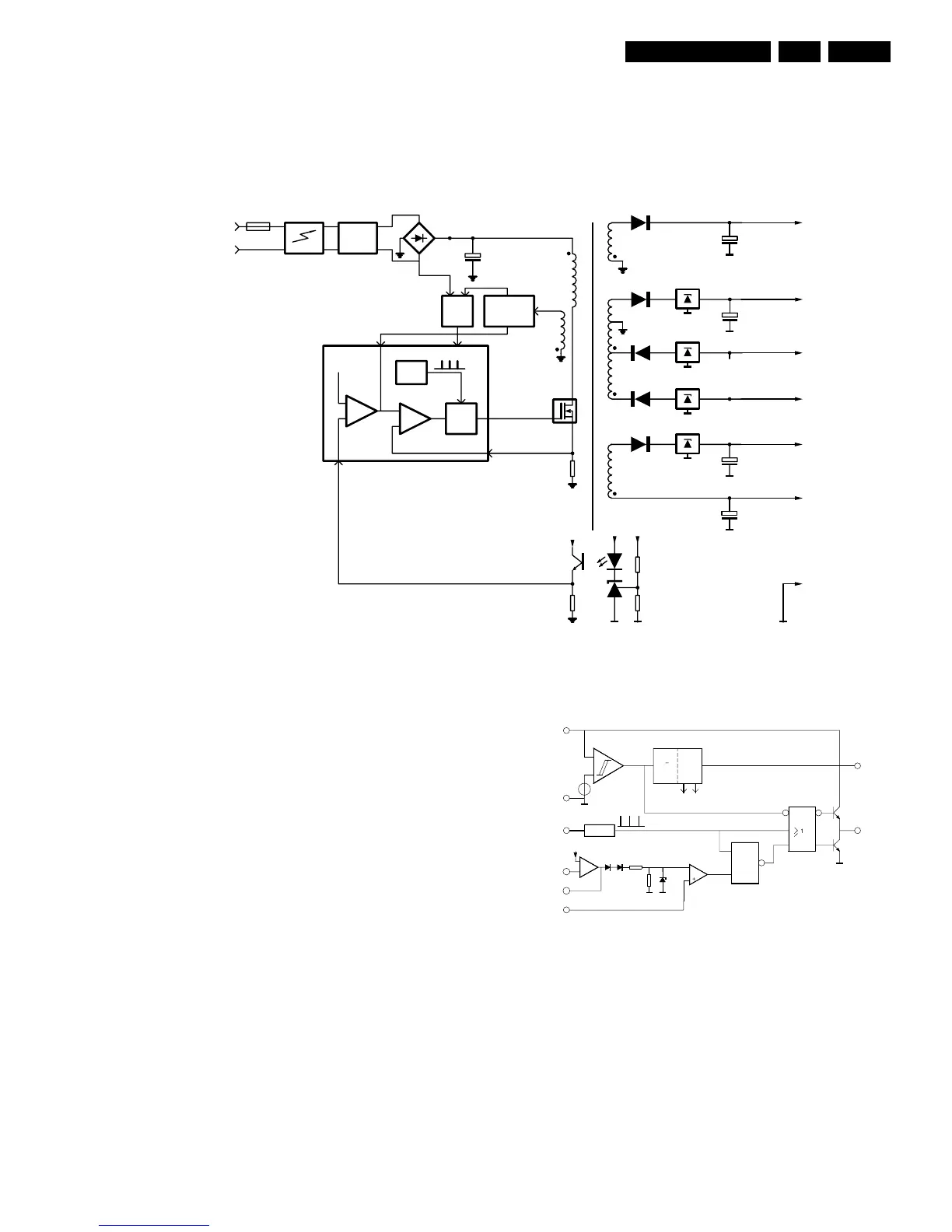
8.2.1 Blockdiagram
Figure 8-10
8.2.2 Function description
MOSFET 7125 is used as a power switch controlled by the
controller IC 7110. When the switch is closed, energy is
transferred from mains to the transformer. This energy is
supplied to the load when the switch is opened. Through
control of the switched-on time, the energy transferred in
each cycle is regulated so that the output voltages are
independent of load or input voltage variations. The
controlling device UC3842 is an integrated pulse width
modulator. A clock signal initiates power pulses at a fixed
frequency. The termination of each output pulse occurs when
a feedback signal of the inductor current reaches a threshold
set by the error signal. In this way the error signal actually
controls the peak inductor current on cycle-by cycle basis.
8.2.3 Description of UC3842
The input voltage Vcc(pin 7) is monitored by a comparator
with hysteresis, enabling the circuit at 16V and disabling the
circuit below 10V. The error amplifier compares a voltage
Vfb(pin 2) related to the output voltage of the power supply,
with an internal 2.5V reference. The current sense
comparator compares the output of the error amplifier with
the switch current Isense(pin 3) of the power supply. The
output of the current sense comparator resets a latch, which
is set every cycle by the oscillator. The output stage is a
totem pole, capable of driving a MOSFET directly
Figure 8-11
8.2.4 Start up sequence
t1: Charging the capacitor at Vcc
C2129 wiil be charged via R3123 and R3134, C2133 and
C2111 via R3129. The output is switched off
During t1.
t2: Charging of output capacitors
When the input voltage of the IC exceeds 14,5V, the circuit is
enabled and starts to produce output pulses. The current
consumption of the circuit increases to about 17mA,
depending on the external loads of the IC. At first, the
7201
7131
6220
6250
6240
6230
6210
5131
7125
2643
Start
Protection
Overvoltage
REGULATION
EMI
FILTER
MAINS
+5V
+5V
+12V
+12V
-8V
VFTD
VDC2
VDC1
0V
RQ
S
CLOCK
+
+
-
-
Vsense
Rsense
v
t2.5V
Error
Amplifier
Verror
PWM
comparator
latch
Vcc
Vcc
Output
Isense
Comp
Vfb
Lightning
Protection
Rectifier
Circuit
CONTROL
2
5
7
9
CL 06532151_018.eps
271100
Figure B : Blockdiagram UC3842
6
8
2.5V
ERROR AMP I SENSE COMP
S
R
7
5
16V
4
OSCRt/ct
GND
VI
2
Vfb
COMP
OUTPUT
Vref
1
LATCH
I sense
1
3
2R
R1V
-
+
+
-
-
+
6V
+
BIAS
S/R
5V
2.5V
REF
CL 06532151_019.eps
271100