Faultfinding Guide
GB 64 CDR7798.
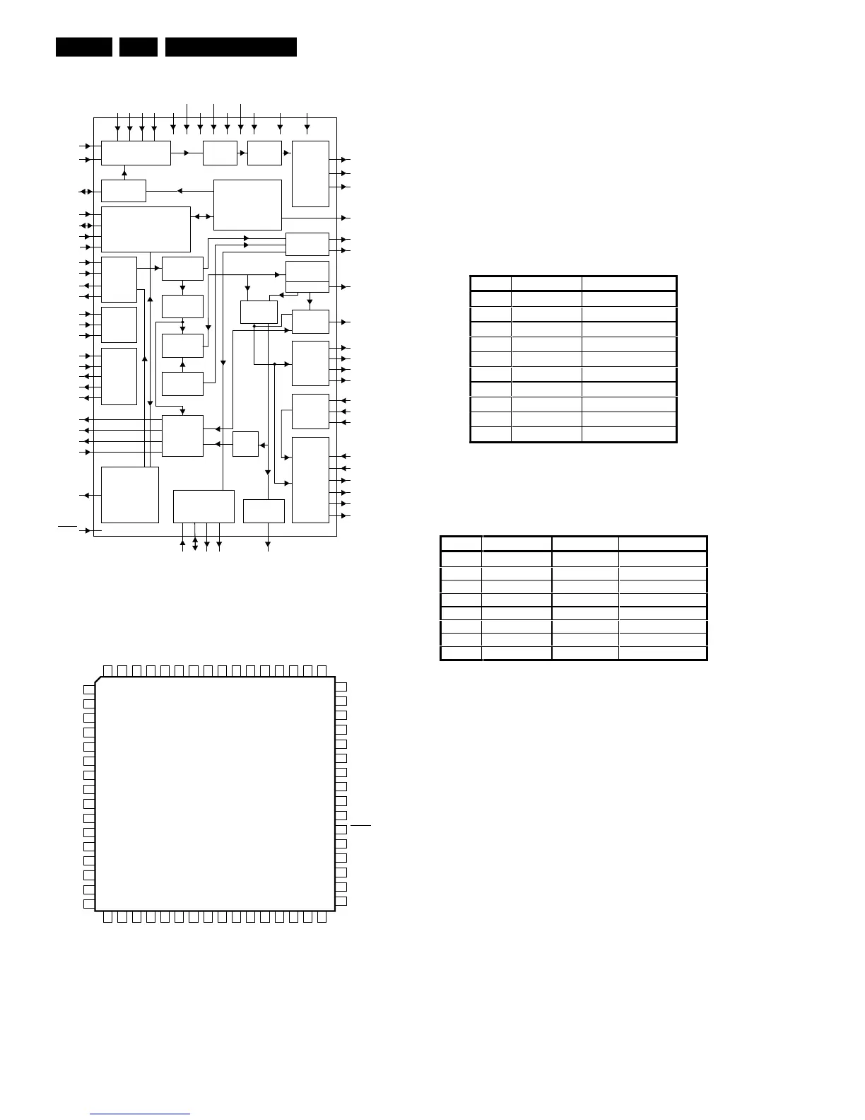
Block Diagram
Figure 8-20
Pin Configuration
Figure 8-21
8.3.4 TDA7073A Power Drivers (7021, 7022)
Description
The TDA7073A is a dual power driver circuit for servo
systems with a single supply. In this configuration it is used
to drive the sledge, tray, focus and radial.
Measurements
Keep microprocessor 7202 in reset by forcing pin 7 of
connector 1208 to +5V. Connect the power supply as
described above in "1.1.1. Supply Voltages". Check the
following voltages :
Figure 8-22
Figure 8-23
8.3.5 BA6856FP Turn Table Motor Driver (7020)
Description
This component is a 3 phase, full wave pseudo linear driving
system with inbuilt Hall Bias circuit and 3 phase parallel
output.
Measurements
Keep processor 7202 in reset by forcing pin 7 of connector
1208 to +5V. The outputs 9, 10, 11 of connector 1006 are 0V.
Pin 21 of the motor driver 7020 is 2.5V ( 10%.
Pin 22 of the motor driver 7020 is 2.5V ( 10%.
Pin 23 of the motor driver 7020 is 0V.
Pin 19 of the motor driver 7020 is 5V ( 10%.
Put the processor out of reset to continue the measurement.
Check MOT1 at pin 59 of CD10. The duty cycle of the output
should be 50%. Check wave form at pin 11 of 7005-D :
amplitude 5V + 5% duty cycle 50%.
The motor driver 7020 can be measured dynamically by
connecting a hall motor to the application panel. Apply a
pulse of 1V 10Hz and 15% duty cycle to pin 22 (Ec) as input
value with reference to pin 21 (Ecr=2.5V). Measure the
output signals on the driver. This will give as response a
square wave on pin 17 and pin 18. When a positive voltage
23
19
18
21
20
EFM
DEMODULATOR
MICROCONTROLLER
INTERFACE
CONTROL
PART
V
ref
GENERATOR
V
RIN
ADC
PRE-
PROCESSING
CONTROL
FUNCTION
OUTPUT
STAGES
R1
R2
12
D1 D2 D3 D4
SCL
SDA
FRONT
END
HFIN
HFREF
ISLICE
I
ref
13
7
40
39
2
1
3
6
TEST
TEST1
25
TEST2
31
TEST3
44
TIMING
SELPLL
24
CRIN
16
CROUT
15
CL16
26
CL11/4
49
8910
V
SSA1
V
SSA2
V
DDA1
V
DDA2
V
SSD1
V
SSD3
V
SSD2
V
DDD1(P)
V
DDD2(C)
4 14 5 17 33 50 58 52 57
RA
FO
SL
54
55
56
LDON
64
DIGITAL
PLL
SRAM
RAM
ADDRESSER
SUBCODE
PROCESSOR
SBSY
48
SFSY
47
SUB
46
RCK
45
STATUS
43
DECODER
MICRO-
CONTROLLER
INTERFACE
RESET
38
VERSATILE PINS
INTERFACE
KILL
BITSTREAM
DAC
RP
RN
22
LP
LN
V
pos
V
neg
36
SDI
35
WCLI
37
SCLI
SERIAL
DATA
(LOOPBACK)
INTERFACE
30
EF
27
DATA
28
WCLK
29
SCLK
SERIAL
DATA
INTERFACE
PEAK
DETECT
EBU
INTERFACE
AUDIO
PROCESSOR
ERROR
CORRECTOR
FLAGS
MOTOR
CONTROL
51
DOBM
53
CFLG
MOTO1
59
MOTO2
60
V1
V2/
V3
V4 V5 KILL
63 34 61 62 32
SILD
42
RAB
41
11
CL96532086_051.eps
080999
1
2
3
4
5
6
7
8
9
10
11
12
13
14
15
16
17
18
19
20
21
22
23
24
25
26
27
28
29
30
31
32
33
34
35
36
37
38
39
40
41
42
43
44
45
46
47
48
51
49
50
52
53
54
55
56
57
58
59
60
61
62
63
64
HFREF
HFIN
ISLICE
V
SSA1
V
DDA1
I
ref
V
RIN
D1
D2
D3
D4
R1
R2
V
SSA2
CROUT
CRIN
VDDA2
LN
LP
V
neg
V
pos
RN
RP
SELPLL
TEST1
CL16
RA
FO
SL
DOBM
SAA7324
V
SSD3
MOTO1
SFSY
SBSY
RCK
SUB
V
SSD1
V5
V4
V2/V3
KILL
EF
DATA
WCLK
V
DDD1(P)
SCLK
TEST3
CL11/4
RAB
SCLI
TEST2
SDI
WCLI
V
SSD2
SILD
MOTO2
STATUS
V
DDD2(C)
CFLG
V1
RESET
LDON
SDA
SCL
CL96532086_052.eps
080999
Pin Location Value
5 7021
12V ± 10%
5 7022
12V ± 10%
1 7022
1.65V ± 10%
2 7022
1.65V ± 10%
6 7022
1.65V ± 10%
7 7022
1.65V ± 10%
1 7021
5.0 ± 10%
2 7021
5.0 ± 10%
6 7021
1.65V ± 10%
7 7021
1.65V ± 10%
CL96532086_053.eps
080999
Pin Location Value DC
9 7022 FOC
5.8V ± 10%
12 7022 FOC 5.8V
13 7022 RAD 5.8V
16 7022 RAD 5.8V
9 7021 SLE 5.8V
12 7021 SLE 5.8V
13 7021 TRAY- 5.8V
16 7021 TRAY+ 5.8V
CL96532086_054.eps
080999