Circuit Descriptions and List of Abbreviations
EN 98 FM249.
Note: There are two versions of this panel, a Basic and an
Enhanced version. Therefore, a lot of components are
therefore not mounted for the Basic version.
For the circuit description, we divide the board into the following
parts:
1. Supply
2. Video processing
3. Audio processing
4. Control
9.4.1 Supply
See figure 'Power Supply Part' in paragraph 9.1.5.
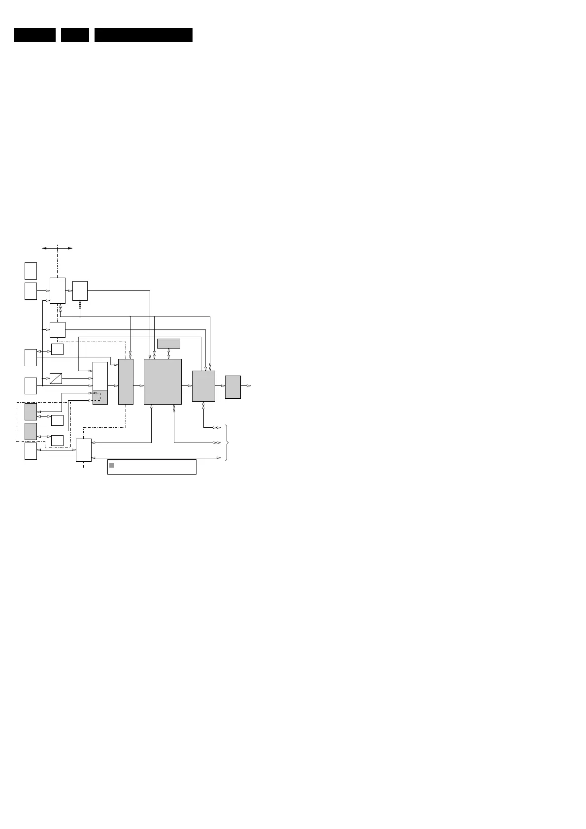
9.4.2 Video Processing (Diagrams SC3, 4, 5, 6, 10, 11 and 12)
Introduction
Figure 9-14 Video path
This mainly consists of a small analogue processing part and
a larger digital signal processing part.
The video inputs like CVBS, YC, High Definition RGB, or YUV
(1fH and 2fH), VGA, and DVI-D are received and processed.
The YPbPr (2fH) is discretely converted to RGB, whereas the
YCbCr (1fH) is processed in the SAA7118 Digital Video
decoder. The base-band video inputs (CVBS and YC) are
output from the digital video decoder as digital YUV, which are
then further processed by the PixelWorks Scaler.
The VGA signals are first AD converted and then processed by
the PW Scaler.
The digital input on the DVI is first decoded by the TMDS
decoder inside the AD9887 and then processed by the PW
Scaler.
The PW Scaler output is going through an EPLD and then via
the LVDS transmitter to the PDP (Plasma Display Panel) as
differential serial data. The PDP is based on ALiS (Alternate
Lighting of Surface) technology and is an interlaced display,
with separate ODD and EVEN fields to be displayed.
Analogue Video
This part describes the analogue video and synchronisation
path of all inputs, until it reaches the 'analogue digital
converters' of either the AD9887 (ADC+TMDS Decoder) or the
SAA7118E (Digital Video Decoder).
Also the switching part is described and the necessary control
signals.
In principle, all video control functions are done by the
PixelWorks processor.
Note: This part also includes the VGA connector panel that is
mounted on top of the SCAVIO panel.
Inputs
There are five video inputs, which are divided in three types:
• VGA (2fH): named VGA1 and VGA2. Both are 15-pole
SUB-D connectors for RGB and HV, and are situated on
the VGA connector panel. For automatic identification by a
PC, each VGA input is foreseen with a DDC NVM IC. VGA2
is set default as loop through of VGA1. In the Enhanced
version, VGA2 can be switched as output, via the control
signals VGA2_OUT and VGA2_EN.
• YPbPr/RGB (combined 2fH and 1fH): named AV3 and
suitable for YCbCr/HD-YPbPr/HD-RGB + HV. These are
cinch inputs. YPbPr and RGB are seen as separate inputs
by the HW and must be properly selected by SW.
• CVBS like (1fH): named AV1 for CVBS and AV2 for Y/C.
These are also cinch inputs.
Video Path
The 1fH signals (including YPbPr) are buffered (item 7113/21/
17) and go directly to a digital video processor, the SAA7118E
(item 7225 on diagram SC5), where they are converted into a
digital signal.
The 2fH signals are also buffered; both YPbPr (item 7074/84/
79) and RGB (item 7141/38/35) buffers get the same input
signals.
When YPbPr signals are connected, the correct input must be
selected, to get a picture with proper colours. Thus, the signals
must pass a video matrix (item 7088/90, see diagram SC3),
where they are converted into RGB. There are two matrices, an
NTSC and an ATSC. With the MATRIX_SEL signal, the correct
matrix is chosen (item 7089). The detection is done automatic,
by an algorithm in the EPLD.
After the matrix, the signals enter a clamp/blanking circuit
(7102/03/04 and 7100), for the removal of the residual sync
signals. The control is done via the lines HD_BLANKN and
HD_CLAMPN coming from the EPLD.
All RGB signals come together at 4-pole switches (item 7146/
58), one for each colour, where they are switched to the AD
converter item 7170 (R_ADC, G_ADC and B_ADC).
Sync Path
All incoming H and V sync signals go to a 4-pole switch (item
7009) where SYNC_SEL and VIDEO_SEL_2 determine, which
signal is available on the ADC.
Before this switch, the VGA sync path is rather straight, only 1
switch (item 7007) is added for the VGA2 sync signals, which
determines if VGA2 sync is input or output (VGA2_OUT).
In the Basic configuration, these switches are omitted, and
replaced by jumpers (4009/4010).
The external sync (AV1 - 3) signals are treated differently. Both
H_HD_EXT and V_HD_EXT go to three circuits:
• A comparator circuitry with an LM319 (item 7025), to
ensure both sync pulses are always positive going (H and
V_SYNC_CMP),
• A level detection circuitry (items 7000 to 7002), to detect if
the sync is of TTL level (H and V_SYNC_TTL),
• A positive/negative going detection circuitry (items 7006 to
7010), to indicate the polarity of the sync in case of TTL
level (H and V_SYNC_POL_N).
All above-mentioned signals go to the EPLD (see diagram
SC11) for further processing.
Processed sync signals H_HD and V_HD coming from the
EPLD, are also switched to the ADC (H_ADC and V_ADC)
along with the proper RGB signals (R_ADC, G_ADC and
B_ADC).
CL 26532038_011.eps
240402
PW164
Pixelworks
AD9887
ADC
+
TMDS
DECODER
2fH
Video+
sync.
switch
TXD/RXD-PW
TXD/RXD-OTC
EPLD
LVDS
to PDP
7670
7656
H+V sync
I2C BUS 1
I2C BUS 2
to OTC (7383)
76057170
7146, 7158
7088, 7090
0375
7025
YPbPr
YUV2fH progressive
15,6 KHz = 1fH
31,2 KHz = 2fH
dig.
I2C BUS 3
RGB
dig.
RGB
dig.
MEMORY
De-int.
digital
processing
path
analogue
processing
path
7280
SAA7118
Dig.
Video
dec.
TMDS
RGB
RGB
7225
CVBS
YC
AV1
AV2
AV3
1fH
sync.
decoder
switch
SWITCH
(SW-
download)
RGB
dig.
RGB
RGB
RGB
DVI-d
HD
Flex
VGA
2
VGA
1
RS
232
NVM
DDC
NVM
DDC
NVM
DDC
! All Functional blocks shaded grey are required for
the"Basic Configuration".
The remainder is required for the "Enhanced Configuration".
www.freeservicemanuals.info
Digitized in Heiloo, Holland