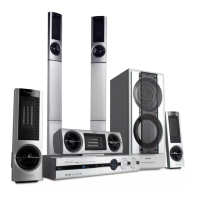
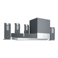
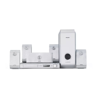
MAIN BOARD
TABLE OF CONTENTS
Internal IC Diagram ................................................... 8-1
Voltages .....................................................................8-2
Circuit Diagram (Top Left) .........................................8-3
Circuit Diagram (Top Right) .......................................8-4
Circuit Diagram (Bottom Left) ....................................8-5
Circuit Diagram ( Bottom Right) ................................8-6
PCB Layout(Top View) ..............................................8-7
PCB Layout(Bottom View) ......................................... 8-8
Electrical Parts list .....................................................8-9
8-1
8-1
ES6128 INTERNAL IC DIAGRAM
EN29F0401 INTERNAL IC DIAGRAM
ES6128
4/16 MB
DRAM
DVD Drive
ROM/Flash
VFD Driver
Audio DAC
T
V Display
Speakers
VFD Panel
Video
EEPROM
A/V Receiver
Vibratto-S
IR Remote
Audio ADC
Microphone In
S/PDIF
M24C02 INTERNAL IC DIAGRAM
WE
CE
OE
State
Control
Command
Register
Erase Voltage Generator
Input/Output Buffers
Program Voltage
Generator
Chip Enable
Output Enable
Logic
Data Latch
Y-Decoder
X-Decoder
Y-Gating
Cell Matrix
Timer
Vcc Detector
A0-A18
Vcc
Vss
DQ0-DQ7
Address Latch
Block Protect Switches
STB
STB