KEY (CONTROL / STANDBY /
VOL) BOARD
TABLE OF CONTENTS
FTD Display Pin Assignment...........................................5-1
Pin Connection ................................................................ 5-1
Circuit Diagram ................................................................5-2
PCB Layout Top View ......................................................5-3
PCB Layout Bottom View ................................................5-3
Electrical Parts List & Voltages ....................................... 5-4
5-1
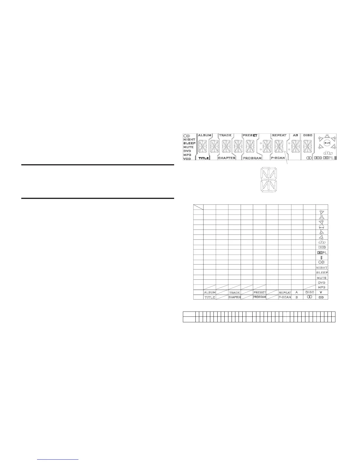
FTD DISPLAY PIN ASSIGNMENT
PIN CONNECTION
## Note ##
1. Fn: Filament pin
2. NP : No Pin
3. NX : No Extended Pin
4. nG : Grid Pin
5. PN : Anode Pin
5-1
PIN NO.
CONNECTION
12345678910111213141516171819202122
31~2332333435
F1
F2 NP
P1P2P3P4P5P6P7P8P9
P10P11P13 P12P14P15P16P17P18
NX9G8G7G6G5G4G3G2G1GF2
F1NPNP
36373839404142434445
NP 10G
a
b
c
d
e
f
g
h
k
p
r
s
m
n
j
(2G - 10G)
Dp
1G 2G3G4G5G6G7G8G9G10G 1G
P2
P1
P3
P4
P5
P6
P7
P8
P9
P10
P11
P12
P13
P14
P15
P16
P17
P18
10G 9G 8G 7G 6G 5G 4G 3G 2G 1G
a
b
c
d
e
f
g
h
j
k
m
p
n
r
s
a
b
c
d
e
f
g
h
j
k
m
p
n
r
s
a
b
c
d
e
f
g
h
j
k
m
p
n
r
s
a
b
c
d
e
f
g
h
j
k
m
p
n
r
s
a
b
c
d
e
f
g
h
j
k
m
p
n
r
s
a
b
c
d
e
f
g
h
j
k
m
p
n
r
s
a
b
c
d
e
f
g
h
j
k
m
p
n
r
s
a
b
c
d
e
f
g
h
j
k
m
p
n
r
s
a
b
c
d
e
f
g
h
j
k
m
p
n
r
s
Col
Dp
Col