30
rl
'--t
t
t_,
t
r
L
t
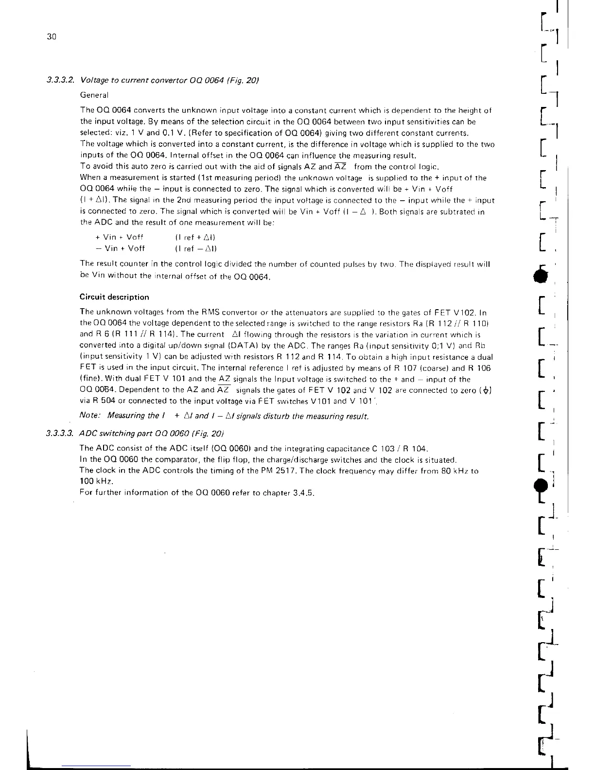
3.3.3.2. Voltage to current
convertor OO 0064
(Fig.
20)
General
The OO
0064
converts
the unknown input voltage into
a constant current
which is dependent to the height
of
the input voltage.
By means of the
selection circuit in the OO
0064
between two input sensitivities can
be
selected: viz. 1 V
and 0.1
V.
(Refer
to
specification of OO
0064)
giving
two
different
constant currents.
The
voltage which is
converted into a constant
current, is the difference in voltage
which is
supplied
to the
two
inputs
of the
OO 0064.
Internal
offset in the OO
0064 can in{luence the measuring
result.
To
avoid this auto zero is
carried oLrt
w,th
the
did
of
srgnals
AZ
aod
AZ from
rhe
con(lol
logic.
When a measurement
is started
(1st
measuring
period)
the unknown voltage is
supplied
to the
+
inputof the
OO 0064 while the
-
input is connected
to zero. The signal
which
is converted
will
be
+
Vin
+
Voff
(l +
Al). The signal in
the 2nd measuring
period
the input voltage is connected to the
-
input
while
the
+
input
is
connected to
zero. The signal which is
converted wil beVin+ Voff
(l
^
).
Both srqna s
are
subtrated
In
the ADC
and the result
of
one measurement
will be:
+
Vin
+
Voff
(l
ref
+
^l)
(l
ref Al)
|-
The
result
counter in the
control logic divided the number
of counted
pulses
bV two. The
displaved result will
be Vin
without
the internai
of{set
of
the OO
0064.
Circuit
descriDtion
The
unknown
voltaqes
from the RMS
convertor or the
attenuators are supplied to the
gates
of FET V 102.
In
theOO0064thevoltagedependenttotheselectedrangelsswitchedtotherangeresistorsRa(R
112
i/
R 110)
and
R
6
(R
111
//
R
114\. The
current
Al {lowing
through
the
resistors
is the väriation in current
which
is
converted into
a
digital
up/down signal
(DATA)
by the ADC. The ranges Ra
(input
sensitivity
0;1 V) and
Rb
(input
sensitivity 1 V)
can be adjusted with
resistors R 112
and
R
114. To obtain a high input resistance a dual
FET
is
used in the input
circuit. The internal reference I
ref is adjusted by means
of
R
107
(coarse)
and
R
106
(fine).
With dual FET V
101
and the
AZ
signals
the Input
voltage is switched
to the
+
and
input
of
the
OO
0064. Dependent to
the
AZ
and AZ
srqnals thp
gares
of
FET
V
102 anrl
V
102
are connected
to zero
(öJ
via
R
504
or connected to
the
input
voltage
via
FET
switches
V101 and V 101'
Note:
Measuring
the |
+
Ll
and I
-
Ll
signals disturb the measuring result.
3.3.3.3.
ADC
switching
part
OO
0060
(Fig.
20)
The ADC consist of the ADC itself
(OO
0060) and
the integrating
capacitance C 103
/
R 104.
In the
OO 0060 the comparator,
the flip
flop,
the charge/discharge
switches and the clock is situated.
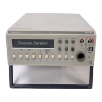
The
clock in the ADC
controls the timing of the
PM
2517. The
clock trequency may differ from
80
kHz to
100
kHz.
For
further
information of the
OQ 0060 reter to
chapter 3.4.5
r
L
t_
t,