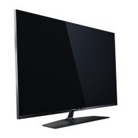
Do you have a question about the Philips Q549.2E LA and is the answer not in the manual?
Details on product information, getting started, user manuals, FAQs, and software drivers.
Information for operating the television set.
Details on various input/output connectors and their pin configurations.
Overview of the chassis structure and layout.
Crucial safety regulations and precautions required during TV set repair.
Explains conventions for resistor, capacitor values, and general schematic notations.
A comprehensive list of abbreviations and their meanings used in the manual.
Explanation of how the third digit of the serial number identifies Bill of Materials variants.
Instructions for proper routing and securing of cables within the set.
Describes recommended positions for servicing the TV set to prevent damage.
Procedures for removing various assemblies and panels, including touch control and signal boards.
Guidance on measuring test points and using test patterns for diagnostics.
Explains different service modes (SDM, SAM, CSM) and the use of ComPair.
Describes the stepwise start-up process and its use in protection state diagnosis.
Details on service tools like ComPair and memory/audio testing.
Introduction to error codes and their role in fault diagnosis.
Procedure for interpreting error codes indicated by the front LED blinking.
Overview of software and hardware protections that trigger fault conditions.
Practical tips for fault finding and repair, covering specific components and issues.
Procedures for upgrading main and standby software via USB.
General conditions and electrical adjustments required for alignment.
How the microprocessor communicates with ICs and uses option codes.
Importance of resetting NVM on repaired SSBs and using ComPair tool.
Introduction to the Q549.2E LA chassis and its predecessor.
Description of the power architecture of the platform.
Key components of the front-end application.
Implementation of the TDA9996 HDMI multiplexer and EDID control.
Details on video and audio processing performed by the PNX8543.
Extension to CI for Conditional Access systems, including CI+ features.
Signal interfacing for the ARM controller and LED drivers.
Block diagram and pin configuration for the DC/DC converter IC.
Block diagram and pin configuration for the Front End IC.
Block diagram and pin configuration for the PNX8543 Stand-by Controller IC.
Block diagram and pin configuration for the Ethernet IC.
Block diagram and pin configuration for the DP83816 Ethernet IC.
Block diagram and pin configuration for the TPA3123D Audio IC.
Wiring diagram for the 32" Elite Core TV model.
Wiring diagram for the 37" Elite Core TV model.
Block diagram illustrating the video signal path and processing.
Block diagram detailing the audio processing path.
Block diagram showing control signals and clock distribution.
Block diagram illustrating the I2C communication paths.
Overview of all power supply lines and their connections.
Circuit diagram for the Ambilight interface and single DC-DC converter.
Circuit diagram for the Ambilight interface and dual DC-DC converter.
Circuit diagram of the Ambilight microcontroller block.
Physical layout of the DC/DC interface board for Ambilight.
Circuit diagram of the Liteon microcontroller block for LED low-power.
Circuit diagram of the Liteon microcontroller block for 8 LED low-power.
Circuit diagram of the Liteon microcontroller block for 10 LED low-power.
Circuit diagram for the PNX8543 Debug interface.
Circuit diagram for the PNX8543 Control signals.
Circuit diagram for the PNX8543 SDRAM interface.
Circuit diagram for the PNX5100 video input interface.
Circuit diagram for the PNX8543 Digital Video In interface.
Circuit diagram for the PNX8543 Audio processing.
Circuit diagram for the PNX8543 Analogue AV interface.
Circuit diagram for the PNX8543 Audio processing.
Circuit diagram for the PNX8543 Analogue AV interface.
Circuit diagram illustrating PNX8543 video streams.
Circuit diagram for PNX8543 digital video output and LVDS interface.
Circuit diagram for the PNX5100 power supply.
Circuit diagram for the PNX5100 SDRAM interface.
Circuit diagram for the PNX5100 video input interface.
Circuit diagram for the PNX5100 power supply.
Circuit diagram for the PNX5100 audio processing.
Circuit diagram for the PNX5100 LVDS interface.
Circuit diagram for the PNX5100 control signals.
Circuit diagram for the PNX5100 debug interface.
Circuit diagram for the FPGA Backlight, LVDS, and I2C-Mux.
Circuit diagram for the FPGA WOW LVDS In/Out module.
Circuit diagram for the FPGA WOW power and control.
Circuit diagram for the FPGA WOW DDR interface.
Circuit diagram detailing the FPGA WOW I/O banks.
Circuit diagram for the Common Interface CI+ PCMCIA connector.
Circuit diagram for the Audio In HDMI interface.
Circuit diagram for the USB connector.
Circuit diagram for the HDMI switch IC.
Circuit diagram for the HDMI switch IC.
Circuit diagram for the PNX8543 flash memory interface.
Circuit diagram for the Ethernet interface.
Circuit diagram illustrating signal buffering.
Circuit diagram for Analogue Externals A.
Circuit diagram for Analogue Externals B.
Circuit diagram for Analogue Externals C.
Circuit diagram for Analogue Externals D.
Circuit diagram for the Mini PCI Connector.
Circuit diagram for the DDR supply.
Circuit diagram for the audio amplifier.
Explanation of SRP symbols and usage in schematics.
SRP list containing signal references for various netnames.
Continuation of the SRP list with more signal references.
Physical layout of the Small Signal Board (top view).
Physical layout of the Small Signal Board (bottom view).
Circuit diagram and layout for the light guide panel.
Physical layout of the guide panel.
Diagram of the Wi-Fi antenna and its layout.
Physical layout of the Wi-Fi antenna.