2002 Jan 17 4
Philips Semiconductors Product specification
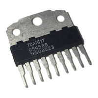
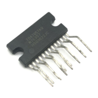
2 × 6 W stereo power amplifier TDA1517; TDA1517P
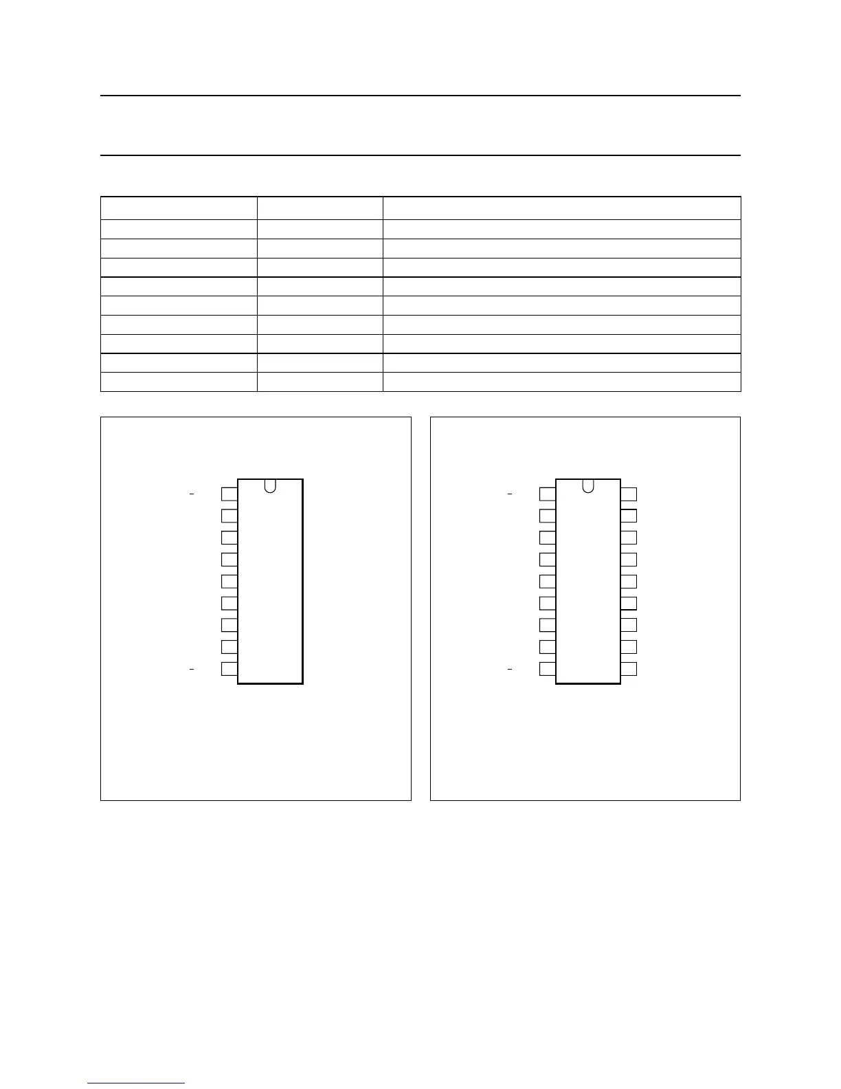
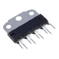
PINNING
SYMBOL PIN DESCRIPTION
−INV1 1 non-inverting input 1
SGND 2 signal ground
SVRR 3 supply voltage ripple rejection output
OUT1 4 output 1
PGND 5 power ground
OUT2 6 output 2
V
P
7 supply voltage
M/SS 8 mute/standby switch input
−INV2 9 non-inverting input 2
Fig.2 Pin configuration for SOT110-1.
dbook, halfpage
MLC352
1
2
3
4
5
6
7
8
9
P
V
OUT2
SGND
INV1
INV2
TDA1517
OUT1
M/SS
SVRR
PGND
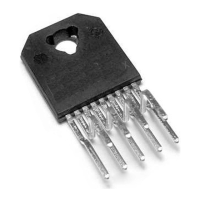
Fig.3 Pin configuration for SOT398-1.
Pins 10 to 18 should be connected to GND or floating.
dbook, halfpage
MLC353
1
2
3
4
5
6
7
8
9
18
17
16
15
14
13
12
11
10
P
V
OUT2
SGND
INV1
INV2
TDA1517P
OUT1
M/SS
SVRR
PGND
FUNCTIONAL DESCRIPTION
The TDA1517 contains two identical amplifiers with
differential input stages. The gain of each amplifier is fixed
at 20 dB. A special feature of the device is the
mute/standby switch which has the following features:
• Low standby current (<100 µA)
• Low mute/standby switching current
(low cost supply switch)
• Mute condition.