Philips Semiconductors
TDA1562Q application note
Koninklijke Philips Electronics N.V.
Application note Rev. 01.02 — 05 May 2006 56 of 62
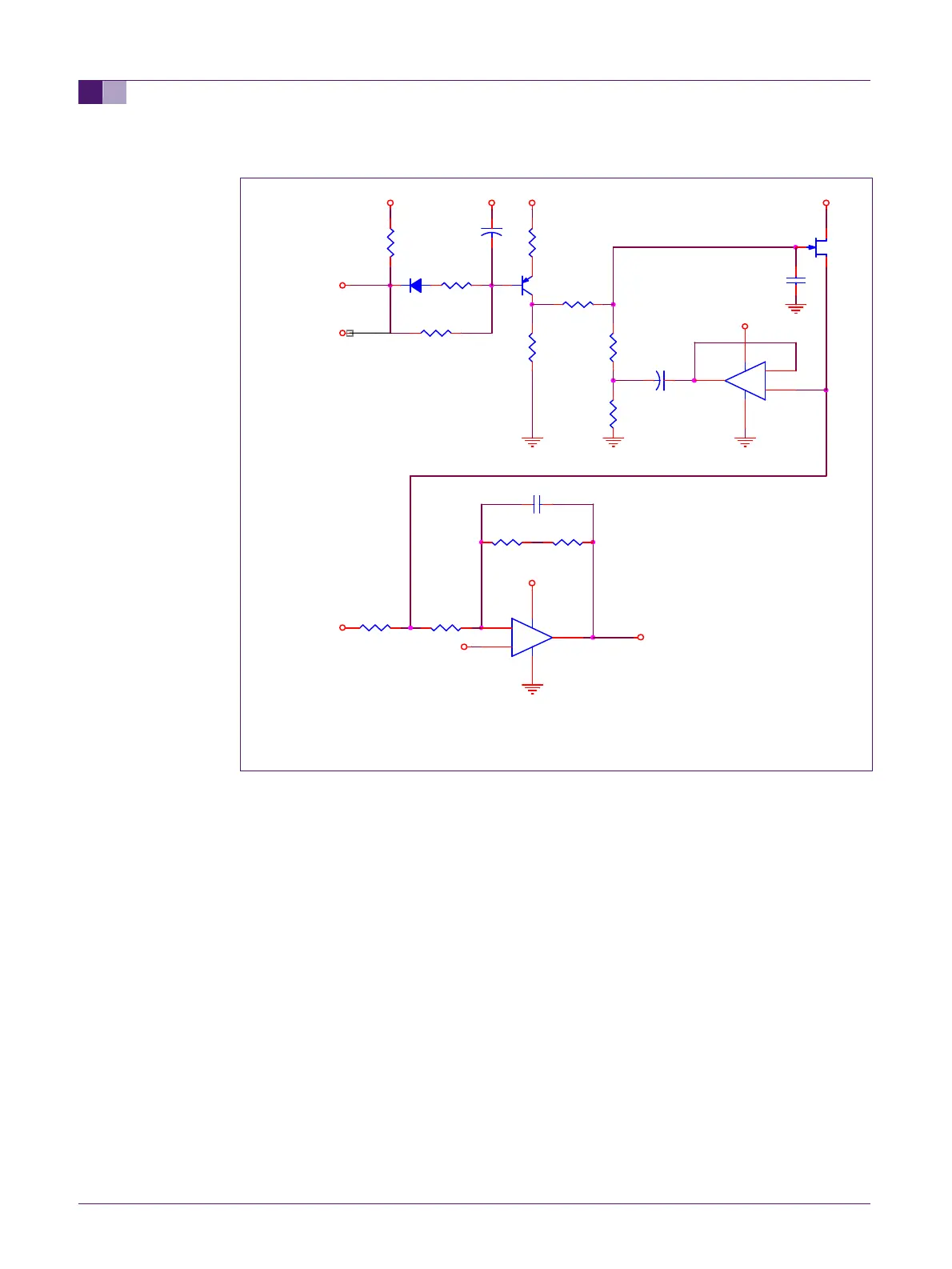
Fig 44. Hard limiter circuit
R1 is the common pull-up resistor for the Open Collector Diagnostic output from any
number of Class H channels. The clipping information is active low.
When a clip occurs, D1 conducts and quickly discharges C1 through R3. The value of R3
sets the attack time and should not be smaller than 4.7k in order to limit Base Current of
Q2.
R2 sets the gain of the feedback loop and the steepness of the limiting knee. R4, R8, R9,
R11 and C2 set up the DC bias and filtering for the Gate of Q1, the special Philips
Semiconductor's FET. The FET is designed to be linear over a wide operating range and
is used in tuners as the AM amplifier. The Drain of the FET is connected to the same
reference voltage used by the audio op amp that inputs the audio signal into the
TDA1562.
The Source of the FET is connected to the Input of the audio op amp and therefore is DC
biased up to the reference voltage (4V). Since the FET is an N channel depletion mode
FET, it is always fully ON and needs to be biased OFF.
By raising the Source pin to the reference voltage (4V) and referencing the GATE
through two parallel paths of 100k + 10k to ground, the GATE sees (-) Vref and is fully
pinched off.
Some of the audio signal is feed back to the GATE of the FET through C4 in order to
linearize the transition area from Pinched Off to just start conducting, in order to linearize
Q2
2N4403
R4 100k min.
Audio input
(comes from pre-amplifier)
to input
of TDA1562
8V 8V 8V Vref (4V)
S
G
D
Vref (4V)
8V
8V
to pin 8 of
TDA1562
(Diagnostic)
to pin 8 of
optional
second TDA1562
(Diagnostic)
R1
100k
R3
4k7 min.
R7 1Meg
R2
100 min.
R8
10k
R9
100k min.
R11
10k
R6
10k
R5
680 max.
R10 680 max.R12 10k
D1
1n4148
C1
1uF/16V
C4 10uF/16V
C2
100pF
C3 100pF
-
+
U1A
OPAMP 1a
3
2
1
8 4
-
+
U2A
OPAMP 1b
3
2
1
8 4
Q1
BF862