Philips Semiconductors
TDA1562Q application note
Koninklijke Philips Electronics N.V.
Application note Rev. 01.02 — 05 May 2006 7 of 62
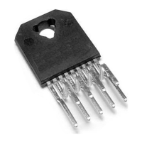
1.4 Pinning
Table 1: Pinning of the TDA1562Q
SYMBOL PIN DESCRIPTION
IN+ 1 Signal input (positive)
IN- 2 Signal input (negative)
C1- 3 Negative terminal of lift electrolytic capacitor 1
MODE 4 Mode select input
C1+ 5 Positive terminal of lift electrolytic capacitor 1
PGND1 6 Power ground 1
OUT+ 7 Positive output
DIAG 8 Diagnostic output (open collector)
Vp1 9 Supply voltage 1
Vp2 10 Supply voltage 2
OUT- 11 Negative output
PGND2 12 Power ground 2
C2+ 13 Positive terminal of lift electrolytic capacitor 2
V
ref
14 Internal reference voltage
C2- 15 Negative terminal of lift electrolytic capacitor 2
STAT 16 Status I/O
SGND 17 Signal ground