Circuit Description and Abbreviation List
EN 38 TE3.1E CA9.
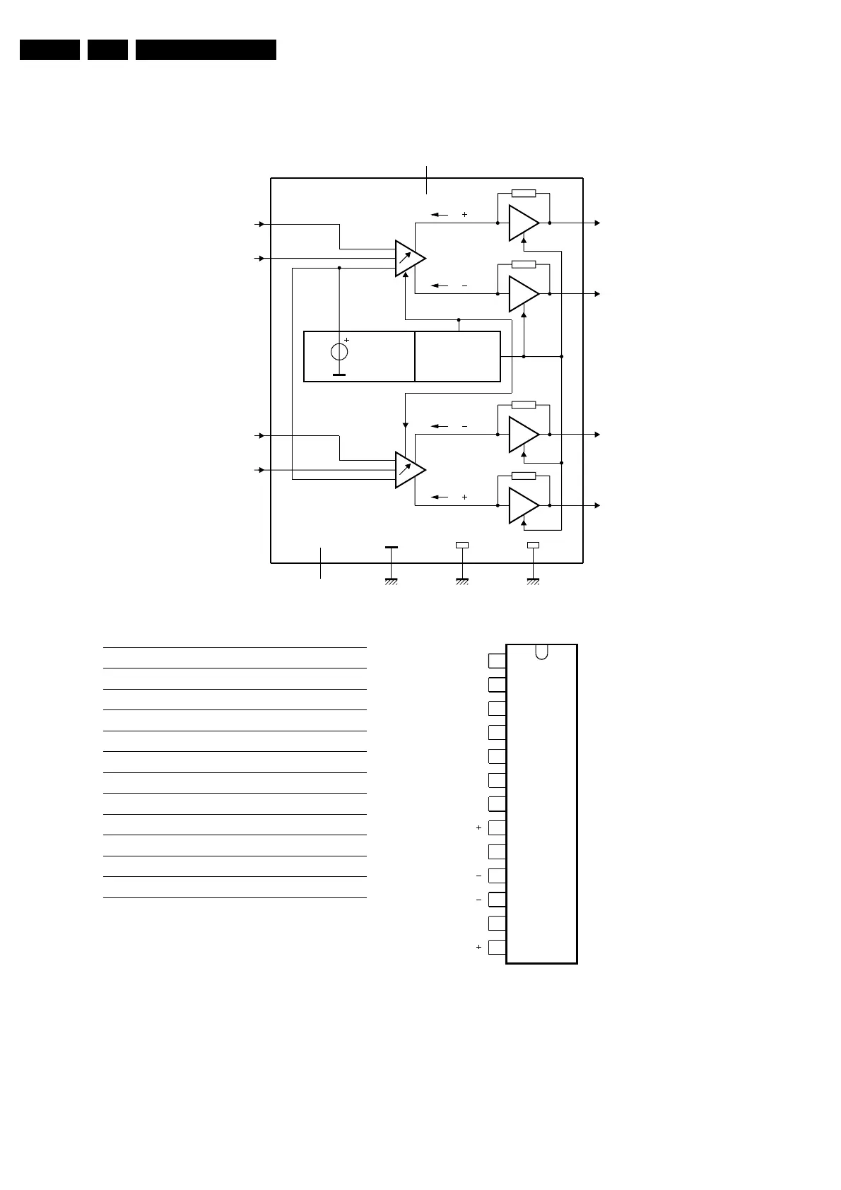
9.4.5 TDA7057A
Figure 9-5 Internal block diagram and pin configuration
Block Diagram
Pin Configuration
F_15160_050.eps
070705
MSA714
I i
I i
Ι
STABILIZER
TEMPERATURE
PROTECTION
V
ref
11
1
3
13
I i
I i
ΙΙ
8
7
5
10
12
power
ground 1
9
power
ground 2
6
signal
ground
2
not
connected
input 1
DC volume
control 1
input 2
DC volume
control 2
TDA7057AQ
4
V
P
positive
output 1
negative
output 1
negative
output 2
positive
output 2
n.c. 2 not connected
V
l (1)
3 voltage input 1
V
P
4 positive supply voltage
V
l (2)
5 voltage input 2
SGND 6 signal ground
VC2 7 DC volume control 2
OUT2+ 8 positive output 2
PGND2 9 power ground 2
OUT2− 10 negative output 2
OUT1− 11 negative output 1
PGND1 12 power ground 1
OUT1+ 13 positive output 1
1
2
3
4
5
6
7
8
9
10
11
12
13
TDA7057AQ
VC1
n.c.
V
P
I (1)
V
I (2)
V
SGND
VC2
OUT2
PGND2
OUT2
OUT1
OUT1
PGND1
MSA716