SECTION 7 - MAINTENANCE INFORMATION
Page 7.3
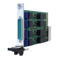
PXI/PXIe LVDT/RVDT/Resolver Simulator Module 41/43-670
pickering
Each channel can be independently veried using the following steps. Results from this verication can be recorded
in the results tables on pages 7.6 to 7.13.
• Outputs A and B of all channels can be connected in parallel, as shown in gure X.X. This is achieved by
grouping all OUTA_S, OUTA_G, OUTB_S, OUTB_G outputs, providing a pair of 2-wire connection to the
DMM.
• For the excitation input connection, the user can either connect the generator to CH1 input (IN_S_1 and
IN_G_1) and use the internal input bus to share the excitation between channels, or parallel all input
connections (all IN_S pins connected to GEN+ and all IN_G pins connected to GEN-) to provide a single
input connection to the generator.
• Using either the GSFP or a custom application, ensure that only the output isolation relays of the chosen
channel are closed. Also make sure the channel under test has a valid input, i.e. the correct input isolation or
input interconnection relays are closed.
• The verication procedure depends on product functionality for 4x-670-1YZ-AABBCC and 4x-670-2YZ-
AABBCC models. For 4x-670-0YZ-AABBCC products, the user can choose to follow VDT or resolver
procedures to verify functionality.
VDT
Gain Verication Procedure
• Setup
1. Close all the required input and output relays
2. Adjust input attenuator
3. Set channel mode to 4-wire
4. Set the % position on both outputs to 100.00
5. Set the maximum output level (VSUM) to its minimum setting according to Table 7.1 to 7.5 (depending
upon the version being tested)
• Procedure
1. Measure the AC RMS voltage on both outputs and record the values
2. Check that the measurements are within the limits indicated by the corresponding table
3. Increase the maximum output level (VSUM) to the next step according to the table, and wait for 1 second
after setting the value
4. Repeat steps 1-3 for every VSUM value on the table. All readings should be within the indicated range
Linearity Verication Procedure
• Setup
1. Close all the required input and output relays
2. Adjust input attenuator
3. Set channel mode to 5/6-wire
4. Set the % position to 0.00
5. Set the maximum output level (VSUM) to its maximum setting (or as high as practically possible)
according to Table 7.6
• Procedure
1. Measure the AC RMS voltage on both outputs and record the values
2. Calculate the measured position as Pos = 100 ∙ (V
A
-V
B
)/(V
A
+V
B
) and check that the measured position is
within the limits indicated by the corresponding table
3. Increase the % position setting to the next step according to the table
4. Repeat steps 1-3 for every position setting on the table. All measurements should be within the indicated
range