PDP-425CMX
179
5678
56
7
8
C
D
F
A
B
E
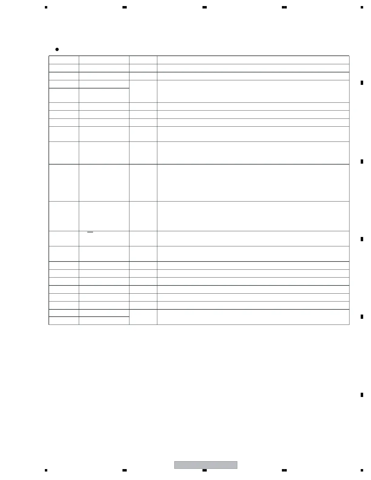
Pin Name I/ONo. Description
AnP I*A Positive LVDS differential data inputs.
AnM I*B Negative LVDS differential data inputs.
Rn,Gn,Bn,
DE,HSYNC,
VSYNC
O
*C
69/71/70
TTL level data outputs. This includes: 16 Red, 16 Green, 16 Blue, and 3
control lines – HSYNC (LP), VSYNC (FLM), DE (Data Enable).
RxCLK INP I91 Positive LVDS differential clock input.
RxCLK INM I92 Negative LVDS differential clock input.
RxCLK OUT O42 TTL level clock output. The falling edge acts as data strobe.
R_FDE I77 Programmable control (DE) strobe select. Tied high for data active when DE
is high.
PLLSEL I5PLL range select. This pin must be tied to V
CC
for auto-range. NC or tied to
Ground is reserved for future use. Typical shift point is between 55 and 68
MHz.
BAL I6Mode select for DC Balanced (new) or non-DC Balanced (backward
compatible) interface. BAL = LOW fornon-DC Balanced mode. BAL = HIGH
for DC Balanced Mode (Auto-detect mode), with this pin HIGH the received
LVDS clock signal is used to determine if the interface is in new or backward
compatible mode (Notes 1) .
DESKEW I4Deskew and oversampling “on/off“ select. Deskew is active when in put is
high. Only supported in DC Balance mode (BAL = High). To complete the
deskew operation, a minimum of four clock cycles is required during
blanking time.
PD
I78 TTL level in put. When asserted (low input) the receiver data outputs are low
and clock out put is high.
STOPCLK O73 Indicates receiver clock in put signal is not present with a logic high. With a
clock input present, alow logic is indicated.
V
CC
I*D Power supply pins for TTL outputs and digital circuitry.
GND I*E
*D : 13, 23, 33, 45, 56, 66
*C : 8–12, 14, 15, 17–22, 24, 26–32, 34, 36–41, 43, 46–53, 55, 57–62, 64, 65, 67, 68
*E : 7, 16, 25, 35, 44, 54, 63, 72
*A : 79, 82, 84, 86, 89, 94, 96, 98
*B : 80, 83, 85, 87, 90, 95, 97, 99
Ground pins for TTL outputs and digital circuitry
PLLV
CC
I2Power supply for PLL circuitry.
PLLGND I1, 3 Ground pin for PLL circuitry.
LVDSV
CC
I
81, 93
Power supply pin for LVDS inputs.
LVDSGND I
76, 88, 100
Ground pins for LVDS in puts.
CNTLE,
CNTLF
O75
74
TTL level data outputs. User-defined control signals - no connect when not
used.
Note 1 : The DS90CF388 is designed to automatically detect the DC Balance or non-DC Balance transmitted data from the DS90C387 and deserialize the LVDS
data according to the defined bit mapping.
Pin Function
[Pin No.]
 Loading...