EasyManua.ls Logo

Pioneer SPEC-2 - Protection Circuit Overview

Pioneer SPEC-2
49 pages
Print Icon
To Next Page IconTo Next Page
To Previous Page IconTo Previous Page
Loading...
4.3
PROTECTION
CIRCUIT
The main
purpose
of the
protection
circuit is
to
protect
the
equipment
and
give
an indication in
the event
of
malfunction, incorrect
operation,
faulty connections,
or other causes.
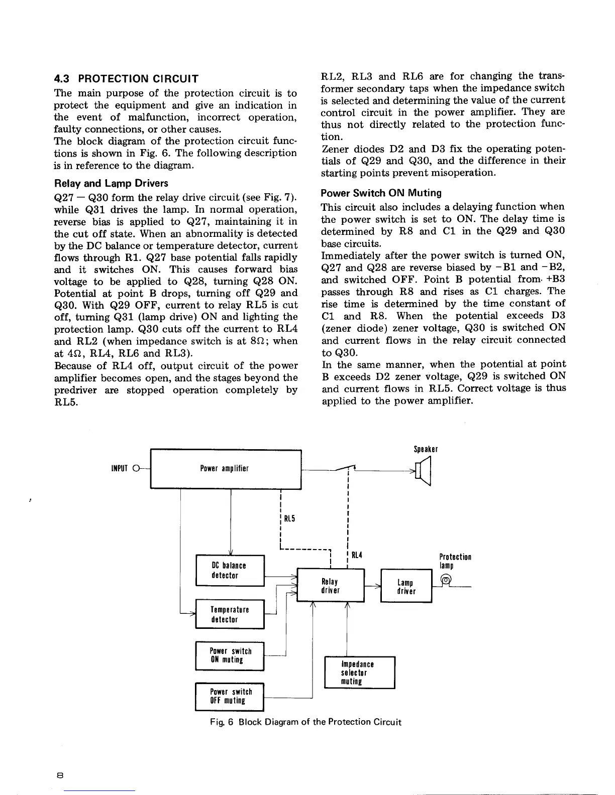
The block
diagram of
the
protection
circuit func-
tions
is shown
in
Fig.
6.
The following description
is
in
reference to
the
dia$am.
Relay and
Lamp Drivers
q27
-
Q30
form
the
relay drive
circuit
(see
Fig.
7).
while
Q31
drives
the
lamp.
In
normal operation,
reverse
bias is applied to
Q27,
maintaining
it in
the cut
off state.
When
an
abnormality
is
detected
by the
DC
balance
or
temperature
detector,
current
flows through
R1.
Q27
base
potential
falls rapidly
and
it switches
ON. This causes
forward bias
voltage
to
be
applied
to
Q28,
turning
Q28
ON.
Potential
at
point
B
drops, turning
off
Q29
and
Q30.
With
Q29
OFF, current to
relay
RL5 is
cut
off, tuming
Q31
(lamp
drive)
ON
and
lighting
the
protection
lamp.
Q30
cuts off the
current to
RL4
and
RL2
(when
impedance switch
is
at
8Q;
when
at
4Q, RL4, RL6 and
RL3).
Because of
RL4
off, output
circuit of the
power
amplifier
becomes open, and the
stages beyond the
predriver
are stopped operation
completely
by
RL5.
RL2,
RLg
and
RL6
are
for
changing
the
trans-
former
secondary
taps
when the
impedance
switch
is
selected and
determining
the
value of
the
current
control
circuit
in the
power
amplifier.
They
are
thus
not directly
related to
the
protectiorr
func-
tion.
Zener
diodes
D2
and
DB
fix
the
operating
poten-
tials
of
Q29
and
Q30,
and the
difference
in
their
starting
points
prevent
misoperation.
Power
Switch
ON
Muting
This circuit
also includes a
delaying
function
when
the
power
switch is set to
ON. The
delay time
is
determined by
R8
and
C1 in the
Q29
and
Q30
base circuits.
Immediately
after the
power
switch
is
turned
ON,
Q27
and
Q28
are
reverse biased by
-B1
and
-B2,
and
switched
OFF.
Point
B
potential
from'+B3
passes
through
R8 and
rises as
Cl charges.
The
rise
time
is determined
by the
time
constant
of
C1 and
R8.
When
the
potential
exceeds
D3
(zener
diode)
zener
voltage,
Q30
is switched
ON
and current
flows in the
relay
circuit
connected
to
Q30.
In
the
same
manner,
when the
potential
at
point
B exceeds
D2 zener
voltage,
Q29
is switched
ON
and
current
flows
in RL5.
Correct
voltage
is thus
applied
to the
power
amplifier.
Fig.
6 Block
Diagram of the
Protection
Circuit

Table of Contents