EasyManua.ls Logo

Pioneer VSX-D409 Service Manual

Pioneer VSX-D409
61 pages
To Next Page IconTo Next Page
Page #1 background imageLoading...
Page #1 background image
ORDER NO.
PIONEER CORPORATION 4-1, Meguro 1-chome, Meguro-ku, Tokyo 153-8654, Japan
PIONEER ELECTRONICS SERVICE, INC. P.O. Box 1760, Long Beach, CA 90801-1760, U.S.A.
PIONEER EUROPE N.V. Haven 1087, Keetberglaan 1, 9120 Melsele, Belgium
PIONEER ELECTRONICS ASIACENTRE PTE. LTD. 253 Alexandra Road, #04-01, Singapore 159936
PIONEER CORPORATION 2000
c
RRV2252
1. SAFETY INFORMATION
......................................
2
2. EXPLODED VIEWS AND PARTS LIST
...............
3
3. BLOCK DIAGRAM AND SCHEMATIC DIAGRAM
.....
8
4. PCB CONNECTION DIAGRAM
.........................
26
5. PCB PARTS LIST
...............................................
39
6. ADJUSTMENT
....................................................
47
CONTENTS
7. GENERAL INFORMATION
................................
48
7.1 DISASSEMBLY
............................................
48
7.2 PARTS
..........................................................
49
7.2.1 IC
............................................................
49
7.2.2 DISPLAY
.................................................
54
8. PANEL FACILITIES AND SPECIFICATIONS
.......
56
T – ZZK JAN. 2000 Printed in Japan
Type
Model
Power Requirement Remarks
VSX-D409 VSX-D309
KUXJI AC120V
KCXJI AC120V
THIS MANUAL IS APPLICABLE TO THE FOLLOWING MODEL(S) AND TYPE(S).
PHONES
MPX
MODE
@ @
MIDNIGHT
2
/DTS
SIGNAL
SELECT
1
R
N∫m-Û≤?/ Digital Signal Processor
AUDIO/VIDEO MULTI-CHANNEL RECEIVER
VSX-D409
VSX-D309
w
w
w
.
x
i
a
o
y
u
1
6
3
.
c
o
m
Q
Q
3
7
6
3
1
5
1
5
0
9
9
2
8
9
4
2
9
8
T
E
L
1
3
9
4
2
2
9
6
5
1
3
9
9
2
8
9
4
2
9
8
0
5
1
5
1
3
6
7
3
Q
Q
TEL 13942296513 QQ 376315150 892498299
http://www.xiaoyu163.com

Other manuals for Pioneer VSX-D409

Question and Answer IconNeed help?

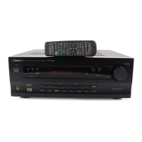
Do you have a question about the Pioneer VSX-D409 and is the answer not in the manual?
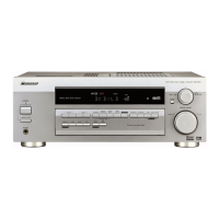
Pioneer VSX-D409 Specifications

General IconGeneral
TypeAV receiver
Channels5.1
Power Output100W per channel
Dolby DigitalYes
DTSYes
AM/FM TunerYes
Input Sensitivity200 mV
Speaker Load Impedance8 ohms
Video ConnectionsComposite
Weight9.5 kg
Digital Inputs2 Optical, 1 Coaxial
Frequency Response5Hz-100kHz

Summary

SAFETY INFORMATION

SAFETY PRECAUTIONS

Precautions for service technicians and customer safety.

PRODUCT SAFETY NOTICE

Notice regarding special safety characteristics of components.

EXPLODED VIEWS AND PARTS LIST

PACKING

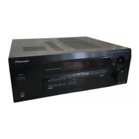
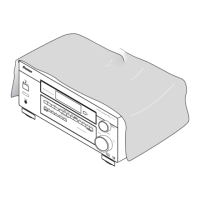
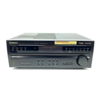
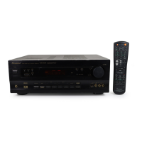
Details of packing contents and accessories for the receiver.

EXTERIOR SECTION

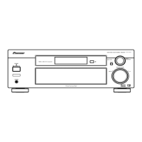
Diagram and parts list for the external components of the receiver.

FRONT PANEL SECTION

Diagram and parts list for the front panel controls and indicators.

BLOCK DIAGRAM AND SCHEMATIC DIAGRAM

BLOCK DIAGRAM

Overview of the receiver's internal signal flow and component connections.

OVERALL WIRING CONNECTION DIAGRAM and AMP INPUT ASSY

Diagram showing how main internal assemblies are interconnected.

D.D & INPUT ASSY (1/3)

Detailed schematic for the Digital/Direct and Input assembly.

D.D & INPUT ASSY (2/3)

Continued schematic for the Digital/Direct and Input assembly.

D.D & INPUT ASSY (3/3)

Final part of the schematic for the Digital/Direct and Input assembly.

AMP&PRIMARY (1/2), TRANS2 and TRANS3 ASSYS

Schematics for amplifier, power supply, and transistor assemblies.

AMP&PRIMARY (2/2), REGULATOR and TRANS1 ASSYS

Schematics for amplifier, regulator, and transistor assemblies.

VIDEO&6CH IN, H. P. and DIGITAL IN ASSYS

Schematics for video input, headphone, and digital interface assemblies.

FRONT, R. ENCODER and POWER SW ASSYS

Schematics for front panel, encoder, and power switch components.

PCB CONNECTION DIAGRAM

DIGITAL IN ASSY

PCB layout and connections for the Digital Input assembly.

TRANS2, TRANS3, REGULATOR and TRANS1 ASSYS

PCB layouts for power supply and regulator assemblies.

AMP INPUT and AMP&PRIMARY ASSYS

PCB layouts for input and amplifier assemblies.

D.D & INPUT ASSY

PCB layout and connections for the Digital/Direct and Input assembly.

H.P., FRONT, R.ENCODER and POWER SW ASSYS

PCB layouts for headphone, front panel, encoder, and power switch.

VIDEO&6CH IN ASSY

PCB layout and connections for the Video and 6-Channel Input assembly.

PCB PARTS LIST

D.D & INPUT ASSY

List of parts for the Digital/Direct and Input assembly.

REGULATOR ASSY

List of parts for the Regulator assembly.

AMP INPUT ASSY

List of parts for the Amplifier Input assembly.

FRONT ASSY

List of parts for the Front Panel assembly.

ADJUSTMENT

GENERAL INFORMATION

DISASSEMBLY

Step-by-step instructions for disassembling the receiver unit.

PARTS

List of components, including ICs, with their functions.

DISPLAY

Information on the FL Display, including pin assignments and grid layout.

PANEL FACILITIES AND SPECIFICATIONS

PANEL FACILITIES

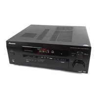
Description and illustration of the front panel controls and indicators.

SPECIFICATIONS

Technical specifications for amplifier, video, and tuner sections.

Related product manuals