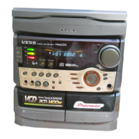
XR-A9800D
50
A
B
C
D
1
23
4
1234
M
PC101
R101
(VNP1661-B)
M
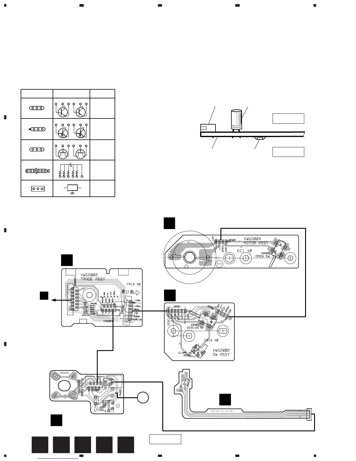
4.1 SW, TRADE, MOTOR, SMEB and FGSB ASSYS
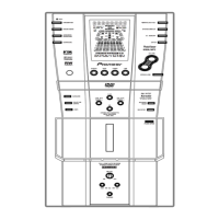
4. PCB CONNECTION DIAGRAM
(VNP1669-A)
(VNP1669-A)
(VNP1669-A)
CN30
F
TRADE ASSY
B
SW ASSY
A
MOTOR ASSY
C
LOADING
MOTOR
NOTE FOR PCB DIAGRAMS :
1. Part numbers in PCB diagrams match those in the schematic
diagrams.
2. A comparison between the main parts of PCB and schematic
diagrams is shown below.
3. The parts mounted on this PCB include all necessary parts for
several destinations.
For further information for respective destinations, be sure to
check with the schematic diagram.
4. View point of PCB diagrams.
Symbol In PCB
Diagrams
Symbol In Schematic
Diagrams
Part Name
B
C
E
D
D
G
G
S
S
B
C
E
BCE
DGS
BCEBCE
BCE
Transistor
Transistor
with resistor
Field effect
transistor
Resistor array
3-terminal
regulator
Capacitor
Connector
P.C.Board
Chip Part
SIDE A
SIDE B
(VNP1722-A)
SMEB ASSY
D
FGSB ASSY
E
CARRIAGE
MOTOR
SPINDLE
MOTOR
SIDE A
A B C D E
 Loading...