Do you have a question about the QMTECH XC7A35T SDRAM and is the answer not in the manual?
Introduces the manual and setup for the core board with Vivado 2016.4.
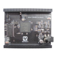
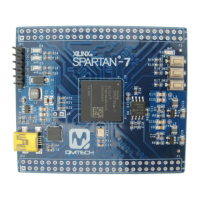
Lists parameters and features of the QM_XC7A35T_SDRAM core board.
Details the required tools for development, including Vivado, USB cable, and power supply.
Describes the hardware design and components of the QM_XC7A35T_SDRAM core board.
Explains the 5V DC input and 3.3V supply for the FPGA, including details on bank power.
Describes the default boot process from external SPI Flash using the N25Q064 memory.
Details the FPGA_DONE status indicator LED (D2) and its connection.
Details the on-board 32MB SDRAM (MT48LC16M16) and its hardware design.
Explains the 50MHz system clock provided by an external crystal.
Describes the two 64-pin headers for extending user modules and IO connections.
Details the 3.3V power supply using the MP2359 DC/DC chip.
Describes the 6-pin JTAG header for connecting to a Xilinx USB platform cable.
Illustrates the PROGRAM_B key and one user key (SW1/SW2).
| FPGA | XC7A35T |
|---|---|
| SDRAM Type | DDR3 |
| FPGA Manufacturer | Xilinx |
| FPGA Family | Artix-7 |
| Logic Cells | 33, 280 |
| DSP Slices | 90 |
| Block RAM | 1, 800 Kb |
| Clock Management Tiles | 5 |
| Operating Temperature | 0°C to +85°C |