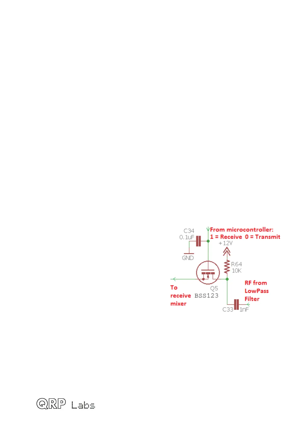
There is also a TX mute switch formed by Q7, another BS170 MOSFET. This was a late
addition to the design: despite all attempts, I could not remove the nasty click on
receive/transmit switching. The mute switch helps to attenuate it. The switch is operated by
the microcontroller Receive/Transmit switch output. When the BS170 switch is on, it has a
low resistance to ground which greatly attenuates the audio signal.
To reduce the audio “thump” when the transceiver is switched from transmit back into
receive, the mute switch needs to remain switched on for a short while after the receiver is
switched back on. A small wait while the thump subsides. This delay is achieved by the R-C
network formed by R60 and C52. This would also introduce a delayed switch-on of the
mute switch, which would allow the thump when switching to transmit to be heard. To
prevent this, diode D5 was added, which bypasses the resistor R60 at the receive-to-
transmit switchover. It ensures that at the receive-to-transmit event, the mute switch is
enabled instantly; but on the transmit-to-receive switchover there is a short delay.
C21 and C22 were originally 10uF electrolytic capacitors. Some constructors experimented
and found that if these capacitors are reduced to 0.1uF the residual Transmit/Receive
switchover click is even further attenuated. However, 0.1uF also reduces the gain of the
receiver chain by 14dB; although overall the receiver has quite high gain, a loss of 14dB
may still be too much particularly on higher frequency bands where the noise levels are
lower. Therefore, the current kit is supplied with 1uF capacitors, which provide the click
attenuation but have negligible effect on the gain.
IC10B is a simple amplifier configured for 41dB of gain. The ½-V mid-rail bias is created by
R39, R40 and C24. Using the 5V power line as “mid-rail” was found to add too much noise.
Finally, IC10A is a simple unity-gain buffer. Although it is just an op-amp it is found to be
perfectly adequate for driving standard earphones.
The effect of the 5K LINEAR (not Log) volume control and the 1K load resistance of the
IC10b input is to create an overall logarithmic characteristic. If you would like a more
aggressive logarithmic characteristic or further analysis and discussion on this topic please
see http://www.qrp-labs.com/qcx/qcxmods/qcxvolume.html
4.9 Transmit signal routing and PA driver
The 74ACT00 is a quad NAND logic gate. The input threshold voltage for a binary “1” is
2.4V which means that the gate is easily switched on by the ~3.3V peak-peak squarewave
output from the Si5351A. The output of the 74ACT00 is 5V peak-peak, perfect for driving
the BS170 MOSFETs in the Class-E PA into saturation.
87
 Loading...