Button pressed Voltage
None 0.00V
“Select” 3.76V
“Rotary” 5.00V
“Exit” 4.55V
In all three cases, the voltage when a button is pressed, is higher than the 3V logic “1”
threshold of the microcontroller. I am able to use a pin-change interrupt to detect that a
button has been pressed, then read the ADC channel 3 and compare the measured voltage
to the table, to determine which button was pressed.
It’s a nice trick for reading multiple buttons on a
single ADC input, and it would work also for a
larger number of buttons! Each one just needs
a different resistor value and eventually, some
care would need to be taken to ensure that the
voltage differences could be read reliably, not
masked by ADC noise or component
inaccuracies. For three buttons, none of these
problems arise.
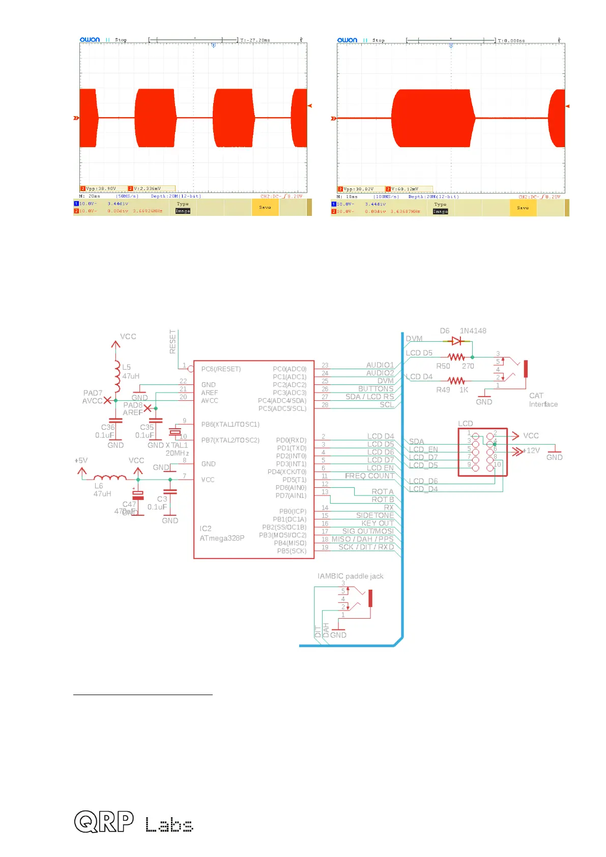
TX/RX Switch control, and Key Out signals
As already discussed, the Key Out signal either
reflects directly the state of a straight key, in
Straight keyer mode, or it is a processed keyer
signal when using the Iambic keyer modes or
Beacon function of the transceiver. The Key
Out signal is generated by the microcontroller
with precise timing in the Beacon and Iambic keyer modes. It is routed to the RF envelope
key-shaping circuit discussed previously.
The Transmit/Receive switch must remain in “transmit” state for a short time after key-up, in
order for the RF envelope of the key-shaping circuit to drop gently down to zero, which
takes approximately 5ms. Due to this, the microcontroller implements a 10ms delay
between key-up and switching the radio back to receive mode.
The diagram (right) illustrates the relationship between these signals, for an example 24
words per minute “dit”. The Key out signal has a “high” period of 50ms exactly. The ramp-
up and ramp-down of the RF envelope has 5 millisecond (approximately) rise and fall times.
The “RX” control line generated by the microcontroller switches on the receiver (allows RF
through to the receive mixer) when it is “high”. It is held in the “low” (transmit) state for 10ms
after key up completes.
The “TX” signal is the inverse of the “RX” signal, and it switches the gate of the audio mute
switch Q7 during transmit. One of the NAND gates IC3D is used as the inverter to create
the “TX” signal from the microcontroller’s “RX” output.
96
 Loading...