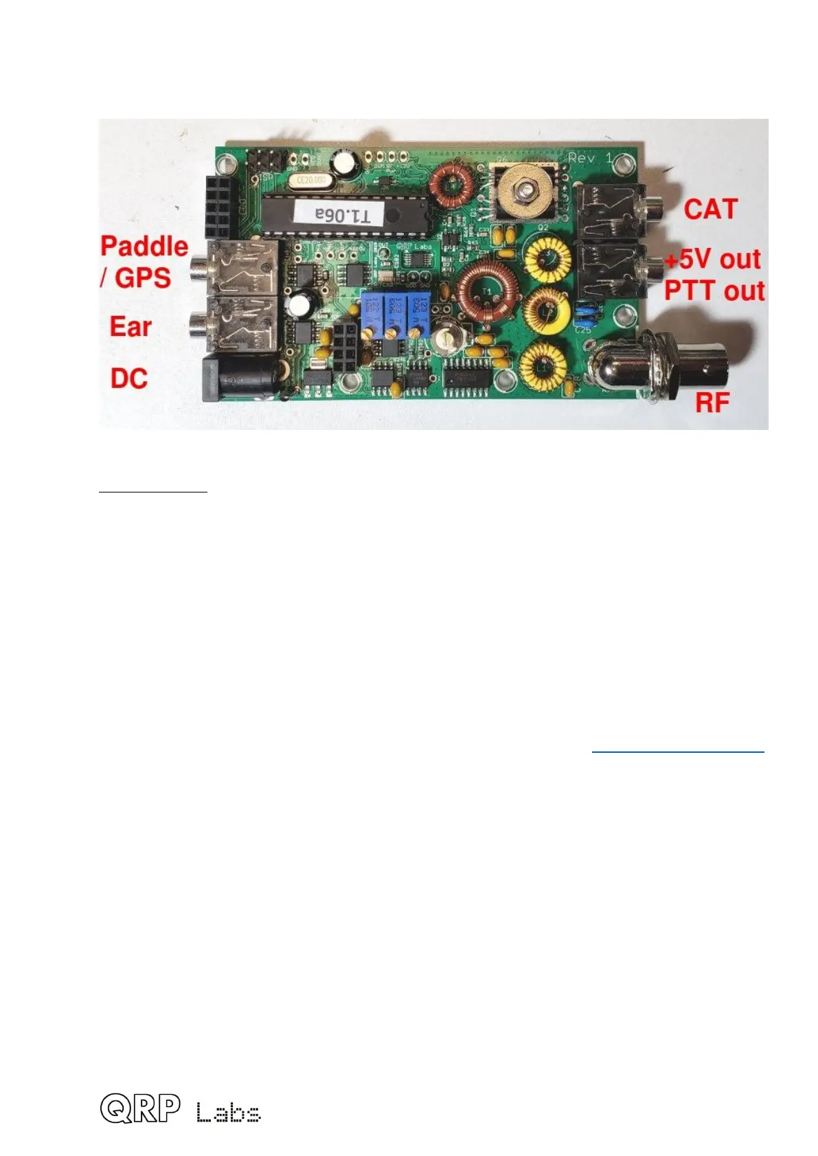
The circuit diagram (schematic) of the main PCB is shown on the previous page. The circuit
diagram of the front panel PCB is shown below. Three 2-row connectors with right-angled
pins on the main PCB connect the two boards; one has 2x5-pins and the other two, 2x3-
pins each.
4.3 Synthesized oscillator
I always start with building the VFO of a radio. It was the hardest thing to get right. How to
get that analogue LC-tuned VFO accurate, free of drift, free of chirp, tuning over the
required range, and with mechanical gearing to be able to make fine frequency
adjustments? A real challenge. Not anymore! Now we have Direct Digital Synthesis (DDS)
ICs and Digital Phase Locked Loop (PLL) ICs, inexpensive and easy to use, that solve all
the problems.
The Si5351A Synthesizer chip used in
this design provides three separate
frequency outputs, with a frequency
range spanning 3.5kHz to 200MHz. The
frequency stability is governed by the
27MHz crystal reference. Pretty stable, in
other words.
The block diagram (right) is taken from
the SiLabs Si5351A datasheet. Briefly, the 27MHz reference oscillator is multiplied up to an
internal Voltage Controlled Oscillator in the range 600-900MHz (the PLL), then divided
down to produce the final output frequency. The multiplication up and the division own are
both fractional and so the frequency
resolution is extremely finely controlled.
The chip has two PLLs and three output
divider units.
For best jitter performance, the Si5351A
datasheet recommends the use of even
integer dividers (no fractional
component) in the MultiSynth dividers
and in this CW transceiver design, this
recommendation is followed.
81
 Loading...