LPWA Module Series
BG77 Hardware Design
BG77_Hardware_Design 38 / 76
For more details about USB 2.0 specification, please visit http://www.usb.org/home
.
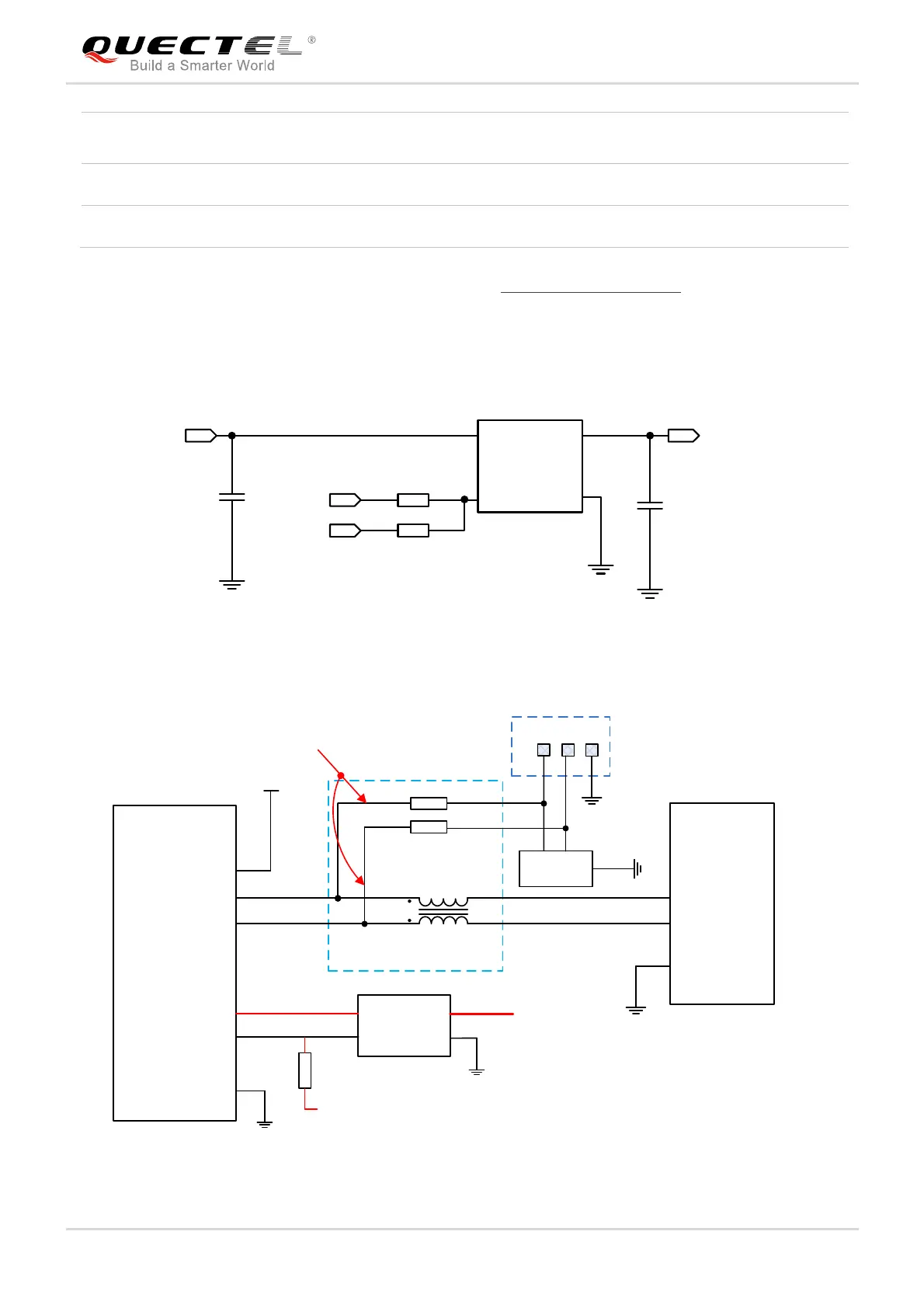
The USB interface is recommended to be reserved for firmware upgrade in customers’ design. The
following figures illustrate reference designs of USB PHY and USB interface.
VI N
EN
VO UT
GND
VBAT
1uF
C1
R1
R2
0R
10 K
VDD_EX T
EXT_PWR_EN
1uF
C2
VDD_USB_3V3
U1
SG M2040-3.3
Figure 15: Reference Design of USB PHY
USB_DP
USB_DM
GND
USB_DP
USB_DM
GND
L1
Close to Module
R1
R2
Test Points
ESD Array
NM_0R
NM_0R
Minimize these stubs
Module
MCU
USB_VBUS
VDD (1.3~1.8V)
USB_VDDA_3P3
LDO
3.3V
VBAT
EN
OUT
IN
GND
EXT_PWR_EN
VDD_EXT
10KR3
Figure 16: Reference Design of USB Interface
USB_VDDA_3P3 42 PI
Power supply for USB PHY
circuit
Vnorm=3.3V
EXT_PWR_EN 64 DO External LDO enable of USB 1.8V power domain
GND 43 Ground