LTE Module Series
EM05 Hardware Design
EM05_Hardware_Design Confidential / Released 34 / 59
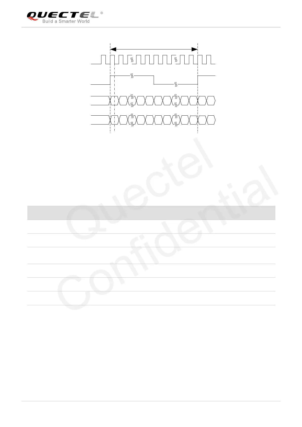
PCM_CLK
PCM_SYNC
PCM_OUT
MSB
LSB
PCM_IN
125us
MSB
1 2 1615
LSB
Figure 21: Auxiliary Mode Timing
The following table shows the pin definition of PCM and I2C interfaces which can be applied on audio
codec design.
Table 11: Pin Definition of PCM and I2C Interfaces
PCM data frame
synchronization signal
Pulled up to 1.8V internally
Pulled up to 1.8V internally
Clock and mode can be configured by AT command, and the default configuration is master mode using
short frame synchronization format with 2048kHz PCM_CLK and 8kHz PCM_SYNC. Please refer to
document [2] about AT+QDAI command for details.

 Loading...