LTE Standard Module Series
EC21_Series_Hardware_Design
105
/ 118
Do not place components on the opposite side of the PCB area where the module is mounted, in
order to facilitate adding of heatsink when necessary.
Do not apply solder mask on the opposite side of the PCB area where the module is mounted, so as
to ensure better heat dissipation performance.
The reference ground of the area where the module is mounted should be complete, and add
ground vias as many as possible for better heat dissipation.
Make sure the ground pads of the module and PCB are fully connected.
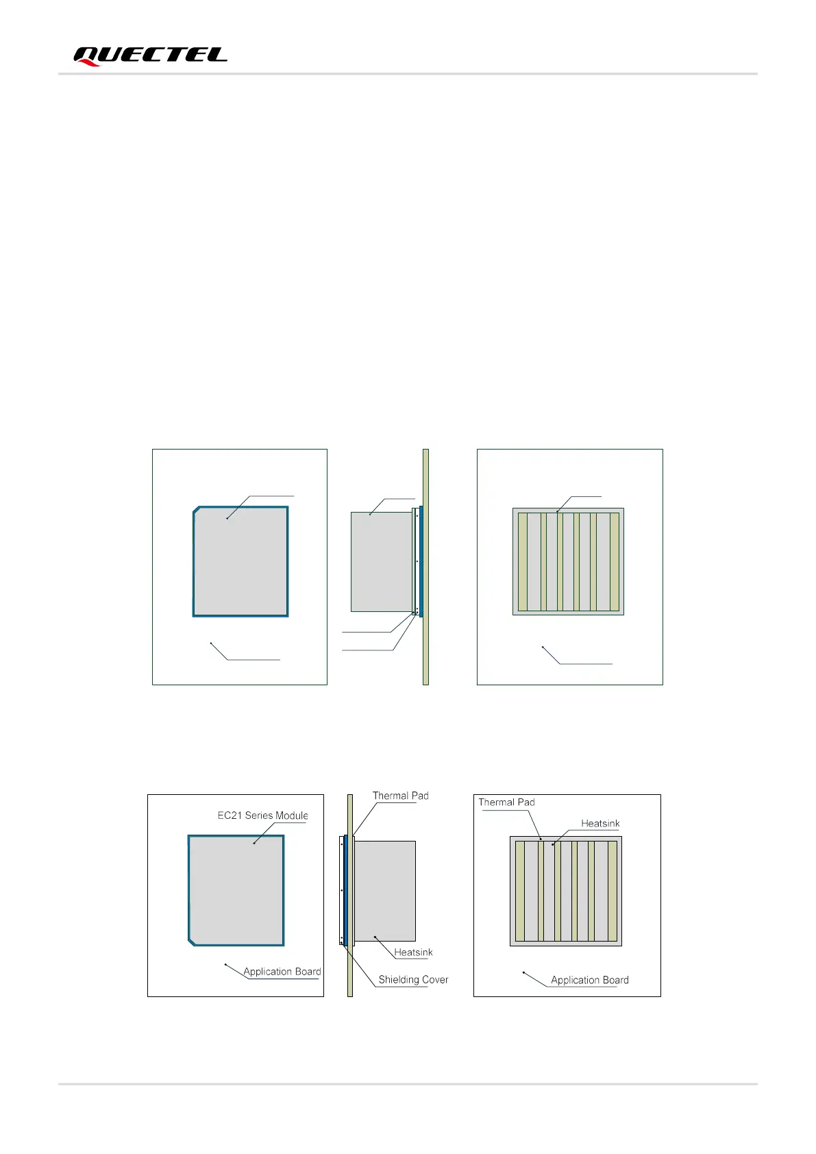
According to customers’ application demands, the heatsink can be mounted on the top of the
module, or the opposite side of the PCB area where the module is mounted, or both of them.
The heatsink should be designed with as many fins as possible to increase heat dissipation area.
Meanwhile, a thermal pad with high thermal conductivity should be used between the heatsink and
module/PCB.
The following shows two kinds of heatsink designs for reference and customers can choose one or both
of them according to their application structure.
Heatsink
EC21 Series Module
Application Board
Application Board
Heatsink
Thermal Pad
Shielding Cover
Figure 42: Referenced Heatsink Design (Heatsink at the Top of the Module)
Figure 43: Referenced Heatsink Design (Heatsink at the Backside of Customers’ PCB)

 Loading...