LTE Standard Module Series
EC21_Series_Hardware_Design
63
/ 118
Table 19: Pin Definition of SGMII Interface
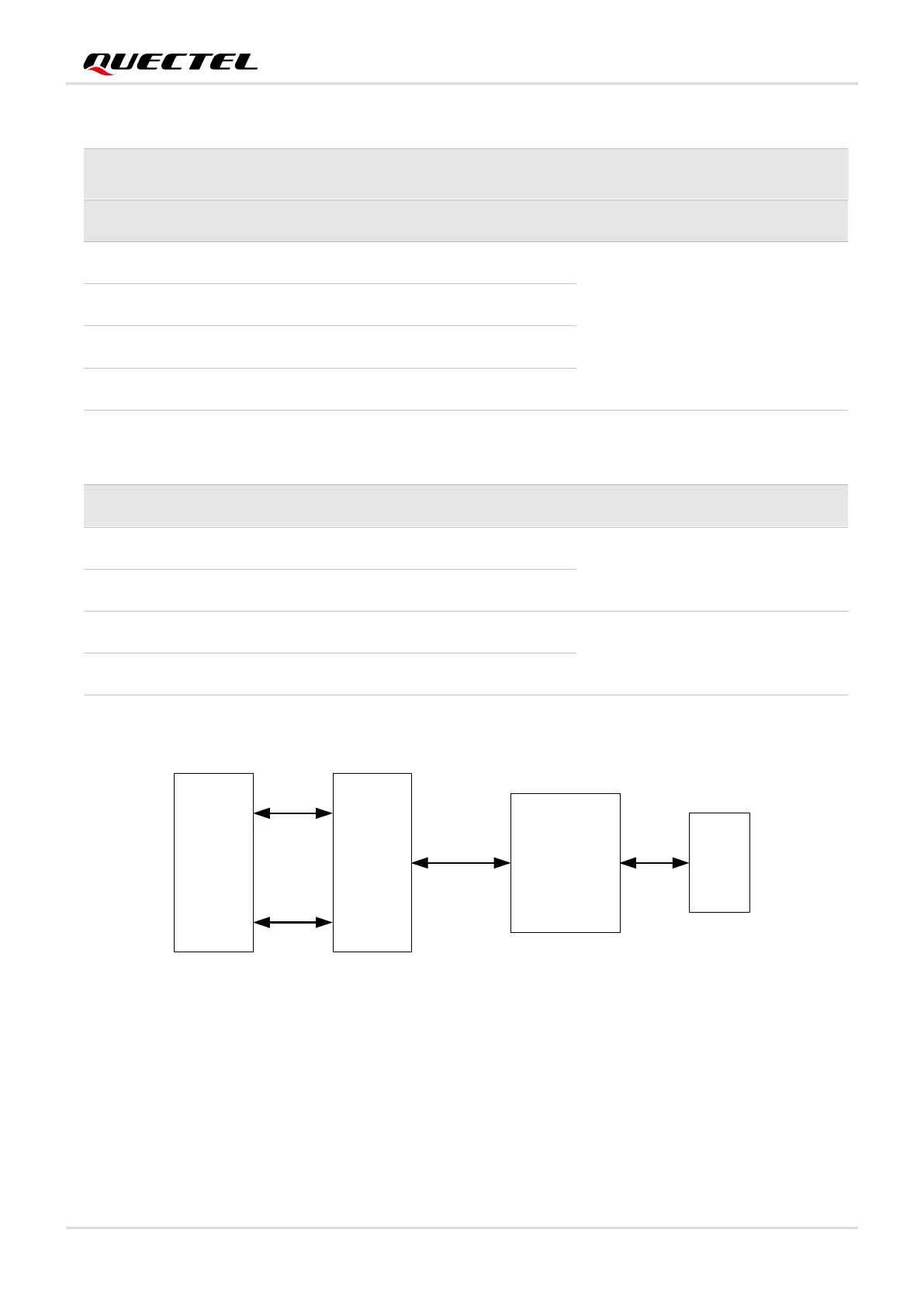
The following figure shows the simplified block diagram for Ethernet application.
Module
AR8033
Ethernet
Transformer
RJ45
SGMII
Control
MDI
Figure 27: Brief Block Diagram for Ethernet Application
The following figure shows a reference design of SGMII interface with PHY AR8033 application.
Pin Name
Pin
No.
I/O Description Comment
Control Signal Interface
EPHY_RST_N 119 DO Ethernet PHY reset
1.8/2.85 V power domain.
If unused, keep them open.
EPHY_INT_N 120 DI Ethernet PHY interrupt
SGMII_MDATA 121 DIO SGMII MDIO data
SGMII_MCLK 122 DO SGMII MDIO clock
USIM2_VDD 128 PO
SGMII_MDATA pull-up power
supply
Configurable power supply.
1.8/2.85 V power domain.
If unused, keep it open.
SGMII Data Interface
SGMII_TX_M 123 AO SGMII transmit (-)
Connect it with a 0.1 μF capacitor,
and close to the PHY side.
If unused, keep them open.
SGMII_TX_P 124 AO SGMII transmit (+)
SGMII_RX_P 125 AI SGMII receive (+)
Connect it with a 0.1 μF capacitor,
and close to the module.
If unused, keep them open.
SGMII_RX_M 126 AI SGMII receive (-)
 Loading...