Renesas RA Family RA4 Quick Design Guide
R01AN5988EU0100 Rev.1.00 Page 49 of 51
Jul.21.21
• Provide sufficient space between routed signals on the same routing layer. Generally, keep a minimum of
one trace width space between signals of the same digital group, and a minimum of 3-5 trace widths
space between signals of different digital groups.
• Provide extra space between clock signals and data signals on the same routing layer. Generally, keep a
minimum of 3-5 trace widths space between clocks and any other digital signals.
• Avoid parallel routing of digital signals on any adjacent routing layers. If signals must be routed on
adjacent signals layers, try to use only orthogonal crossings wherever possible.
If possible, separate PCB signal layers using power or ground layers between signal layers. The solid copper
of the power or ground layer can act as a "shield" for the digital signals.
Each standardized interface will have specific requirements. To ensure that the PCB is designed to avoid
signal crosstalk problems, it is strongly suggested to refer to the relevant standards for each interface in the
design.
15.3 Signal Group Selections
Some pin names have an added _A, _B, or _C suffix to indicate signal groups. When assigning certain
peripheral functions, such as IIC, SPI, SSIE, ETHERC, and SDHI, select the functional pins having the same
suffix. In some cases, the AC timing characteristics shown in the "Electrical Characteristics" chapter of the
Hardware User's Manual are measured for each signal group. If the signal groups are mixed, the peripheral
is not guaranteed to function and the stated AC timing characteristics may not apply.
If the pin names for a peripheral function to not have a signal group suffix, it is safe to select the most
convenient pin assignment for each function signal.
Refer to the sections "Peripheral Select Settings for each Product" and "Notes on the PmnPFS Register
Setting" in the "I/O Ports" chapter of the Hardware User's Manual.
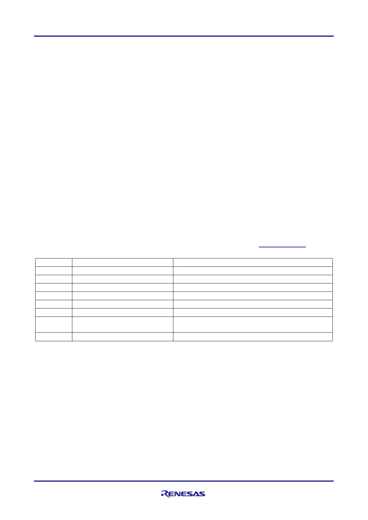
16. References
The following documents were used in creating this Quick Design Guide. Visit the Renesas website for the
latest version of each of these documents.
Renesas RA4M1 Group, User’s Manual: Hardware
Renesas RA4M2 Group, User’s Manual: Hardware
Renesas RA4M3 Group, User’s Manual: Hardware
RA Arm
®
TrustZone
®
Tooling Primer
Security Design with Arm
®
TrustZone
®
- IP Protection
Securing Data at Rest Using the Arm
®
TrustZone
®
Establishing and Protecting Device Identity using SCE9
and Arm
®
®
Device Lifecycle Management Key Installation

 Loading...


