Renesas RA Family RA4 Quick Design Guide
R01AN5988EU0100 Rev.1.00 Page 37 of 51
Jul.21.21
10.2.1 Internal Pull-Ups
• Most pins on ports 0 through 9 have the option of enabling a pull-up resistor. The pull-up is controlled by
the Pull-Up Control (PCR) bit in each Port mn Pin Function Select (PmnPFS) Register. The PCR bit in
each PmnPFS register controls the corresponding pin on the port.
• The pin must first be set as an input with the associated bit in the PmnPFS register. Set the PCR bit to “1”
to enable the pull-up and to “0” to disable it.
• After reset, all PCR registers are cleared to “0”, so all pull-up resistors are disabled.
• The pull-up is automatically turned off whenever a pin is designated as an external bus pin, a GPIO
output, or a peripheral function output pin.
10.2.2 Open-Drain Output
• Pins configured as outputs normally operate as CMOS outputs.
• Most pins on ports 0 through 9 have the option of being configured as an NMOS open-drain output.
• The N-channel open-drain control (NCODR) bit in each Port mn Pin Function Select (PmnPFS) Register
controls which pins operate in open-drain mode. Setting the applicable bit in each register to a “1” makes
the output open-drain. Setting the applicable bit in each register to a “0” sets the port to CMOS output.
10.2.3 Drive Capacity
Most pins on ports 1 through 9 have the option of enabling an output drive capacity. For Arm Cortex-M4
devices, the drive capacity can be set to low- or middle-drive capacity. For Arm Cortex-M33 devices, the
drive capacity can be set to low-, middle- or high-drive capacity.
• The drive capacity switching is controlled by the Drive Capacity Control Register (DSCR) bits in each Port
mn Pin Function Select (PmnPFS) register.
• After reset all DSCR registers are cleared to 0 therefore all pins are set to low drive output. Setting a
value other than “00” will change the drive capacity of the output for the selected pin.
• The maximum total output of all pins summed together is 60 mA for Arm Cortex-M4 devices or 80 mA for
Arm Cortex-M33 devices.
• The typical differences the drive levels are shown below. Actual output current levels vary by device and
pin type. See the specific MCU User Manual for details.
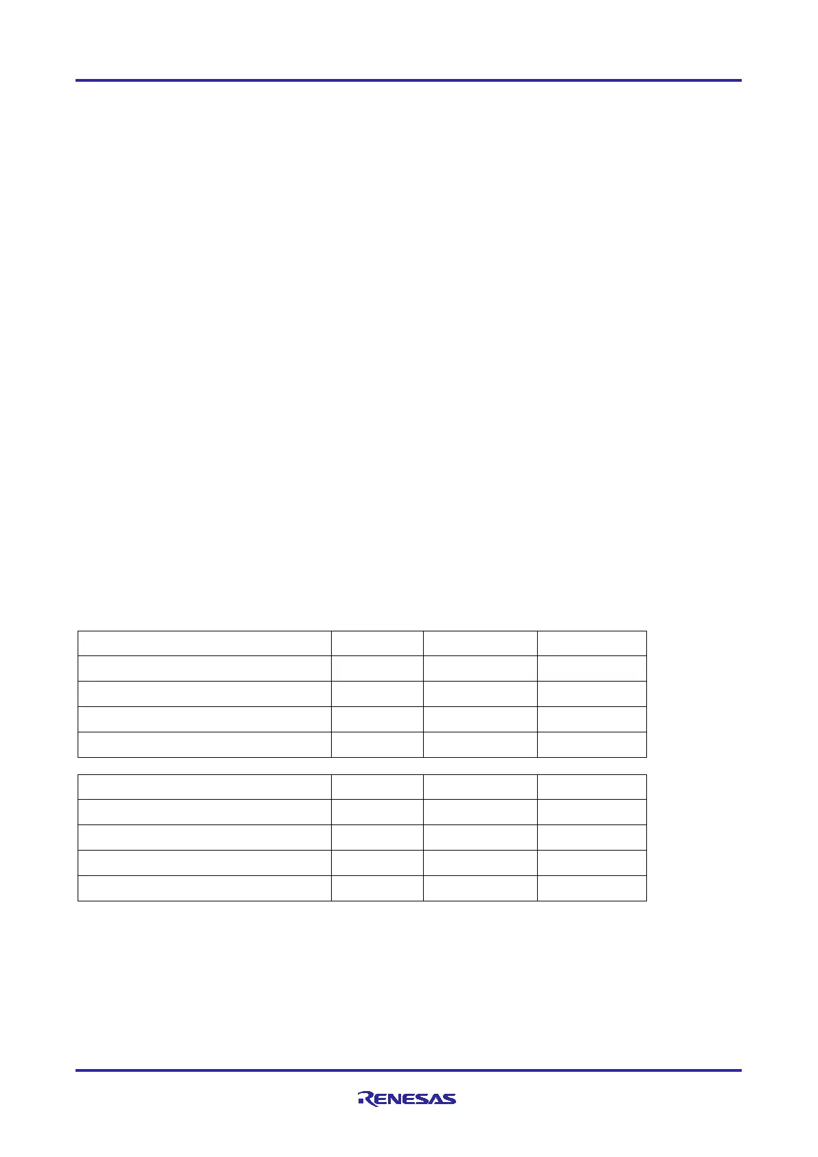
Table 15. Pin Drive Capacity
Typical output pins DSCR[1:0] Drive Capacity Max (mA)
Permissible output current per pin 0 0 Low Drive 4.0
Permissible output current per pin 0 1 Middle Drive 8.0
Invalid setting; do not use 1 0 -
Permissible output current per pin 1 1 High Drive 32
High drive output pins DSCR[1:0] Drive Capacity Max (mA)
Permissible output current per pin 0 0 Low Drive 4.0
Permissible output current per pin 0 1 Middle Drive 8.0
Invalid setting; do not use 1 0 -
Permissible output current per pin 1 1 High Drive 40
Output drive capacity can have a significant impact on overall performance of a board design. The following
points should be considered when selecting the drive capacity for each output.
• It is recommended to start with all pins set to low-drive capacity (default) and evaluate the performance.
• Depending on the board layout, pins set to middle- or high-drive capacity may result in higher EMI
radiation.
• Long traces may require higher drive capacity for signals to propagate correctly to the receiver.

 Loading...


