1
1
2
2
3
3
4
4
5
5
A A
B B
C C
D D
Title
Size Document Number Rev
Date: Sheet of
240191002 1.0
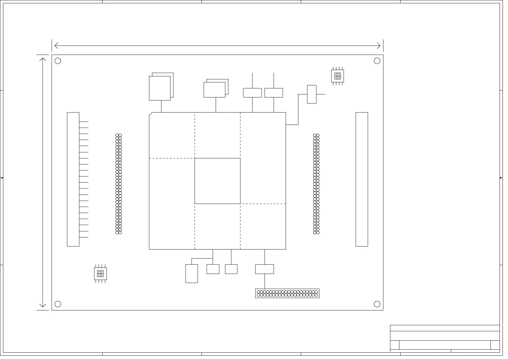
RH850(mango) D1M2H Adapter Board
A3
2 13Friday, June 02, 2017
RH850(mango) D1M2H Adapter Board Block Diagram
BLOCK DIAGRAM
180mm
120mm
GND
DDR2SDR
P1
P2
JP0
P0
P40
P10
P11
P44
P45
P16
P17
P43
P46
P47
P21
P42
1G x2
+3.3V
P0 LIN,CSI,TIMER,RTC
P1 CSI,TIMER,ADC
P2 CSI,TIMER,PWM,IIC
P3 TIMER,PWM,PCM,ETHER,SG,SSIF,IIC,ADC
P10 TIMER,ADC
P11 TIMER,ADC
P16 TIMER,PCM,MOTOR,ZPD
P17 TIMER,PCM,MOTOR,ZPD,ADC
P21 TIMER,SFLASH,MLB
P40 VDCE0(MIPI)
P42 CSI,TIMER,ADC,PWM,IIC,ETHER,SG,VDCE0
P43 VDCE0,VDCE1,TIMER,LCD
P44 LIN,CSI,TIMER,VDCE0,PWM,LCD
P45 CSI,TIMER,ADC,VDCE0,PWM,LCD
P46 VDCE0,VDCE1,ETHER
P47 VDCE1,ETHER
JP0 LIN,TIMER,RTC,JTAG
32.768Khz
ISOVDD
REG0VCC
REG1VCC
OSCVCC
SFVCC
A0VCC
+5V
8Mhz
DDR2
(16bit)
512M x2
SERIAL FLASH
BNC
EVCC
RVCC
ZPDVCC
PLLVCC
TP TP
+12V
B0VCC
B1VCC
B2VCC
B3VCC
B4VCC
ISMVCC
MVCC
BSW
RSDS
BSW BSW
ETHER ETHER
BSW
VI1 ITU
DSW
P3
DSW
 Loading...


