Do you have a question about the Samsung PS42C7HX/XEC and is the answer not in the manual?
General safety precautions to avoid electric shock, radiation, and physical damage.
Precautions for service personnel during repairs, including ESD and capacitor discharge.
Guidelines for handling ESD-sensitive parts to prevent static discharge damage.
Precautions for product installation, including carrying, ventilation, and antenna connection.
Lists key features of the TV, including RF, Power, Video, Sound, PDP Module, and Remocon components.
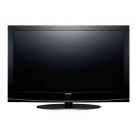
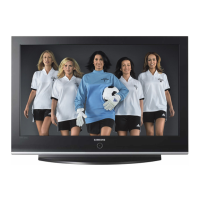
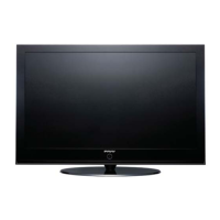
Details on model, screen size, dimensions, weight, color system, sound system, and inputs/outputs.
Comparison of specifications between different models (PS-42C7H vs. Puccini(V4)).
Lists supplied accessories and optional accessories that can be purchased.
Before Performing After Sales Services - Check equipment, workspace, and pad.
Instructions for entering and exiting service mode using general and factory remotes.
Details on Calibration, Option Table, and White Balance settings for factory data.
Specific adjustment parameters like SVP-PX, Option Block, STV8257/STA323W, YC Delay.
Instructions on how to update the Flash ROM using the Flash Downloader.
List of replaced items, their codes, and check items after replacement.
SMPS panel voltage adjustment procedures for Vs, Va, Vset, Ve, Vscan.
Exploded view and part list for the PS42C7HX/XEC model.
Service item list for PS42C7HX/XEC, including Assy code, code number, description, and specification.
Initial checks for troubleshooting, including cable connections and power input.
Troubleshooting steps for various error modes like No Power, No Sound, No Picture.
Lists Assy codes, descriptions, and major symptoms for troubleshooting by component assembly.
High-level block diagram showing the main functional blocks of the TV.
Block diagrams of specific sections like Main Board, DC-DC SMPS, Driver Boards, Logic Board, Power.
Overall wiring diagram showing connections between major boards and components.
Partial wiring diagrams detailing connections between PDP modules and SMPS.
PCB layout of the Main Board, identifying key ICs and their functions.
PCB layout and components of the Power & IR Board.
PCB layout of the Function Board.
PCB layout of the Side AV Board, showing input jacks.
PCB layout of the Main SMPS Board, including AC input and connector pinouts.
PCB layout of the DC-DC SMPS Board, including connector pinouts and test points.
PCB layout of the PDP Module, identifying logic, X, Y, buffer, and address boards.
Analog schematic diagram showing power supply circuits and voltage distribution.
Schematic diagram of the MICOM section, including main and sub-MICOMs, and flash memory.
Schematic diagram for various input/output jacks like SCART, COMPONENT, AV, PC, and SERVICE.
Schematic diagram for the HDMI input and DVI signal interface.
Schematic diagram for the sound section, including sound amplifier and noise solution circuits.
Schematic diagram of the SVP-PX scaler IC, DDR memory, and power supply.
Schematic diagram of the DTV Tuner module, including connections and RF stages.
Schematic diagram for the function buttons and FBE control.
Schematic diagram related to FBE (Frame Buffer Enhancer) options.
Schematic diagram for the FRC (Frame Rate Control) section.
Schematic diagram showing FRC memory connections.
Schematic diagram for LVDS transmission from LBE and FRC to logic.
Schematic diagram for DTV module connection, tuner, and power interface.
Overview of front and side panel controls and speaker connections.
Description of rear panel connections and ports.
Detailed explanation of remote control buttons and their functions.
Notes and precautions regarding wall bracket installation and mounting kits.
Step-by-step guide for assembling the wall mount bracket.
Procedures for securely mounting the TV set to the wall bracket.
Guide on how to adjust the TV's mounting angle after installation.
Instructions on connecting external devices to the PDP TV.
General notice and procedures for disassembling and reassembling the unit.
Steps to separate the ASSY BRACKET P-TERMINAL.
Steps to separate the ASSY PCB MISC-MAIN.
Steps to separate the BRACKET-PCB.
Steps to separate the FILTER-EMI AC LINE.
Steps to separate the ASSY BOARD P-SIDE AV.
Steps to separate the SHIELD CASE.
Steps to separate the ASSY BRACKET P-WALL.
Steps to separate the ASSY SPEAKER P.
Steps to separate the ASSY BOARD P-POWER&IR.
Steps to separate the ASSY PCB P-SMPS & SMPS DC-DC.
Steps to separate the ASSY PDP MODULE P-LOGIC MAIN BOARD.
Steps to separate the ASSY PDP MODULE P-X MAIN BOARD.
Steps to separate the ASSY PDP MODULE P-Y MAIN BOARD.
Steps to separate the ASSY PDP MODULE P-ADDRESS BUFFER BOARD.
Timing diagram illustrating the power ON/OFF sequence and voltage signals.
Detailed description of the Main SMPS, including outline, input, output, and protection features.
Description of the PDP module's logic board, including components and functions.
Definition and mechanism of the X, Y drive circuits for PDP pixel control.
Description of the function of each board in the drive circuit.
Details on drive waveforms and the function of each pulse (Preset RA, Main RA, Scan, IDS, CPS, CMS).
Explanation of FET operation and high-voltage switching mechanism.
Discussion of issues like screen burn-in, cable length, and digital/analog broadcast reception.
Definitions of various technical terms used in the manual, like Virtual Channel, Dolby Digital, etc.
| Screen Size | 42 inches |
|---|---|
| Display Technology | Plasma |
| Resolution | 1024 x 768 |
| Contrast Ratio | 10000:1 |
| HDMI Ports | 2 |
| Brightness | 1500 cd/m² |
| Response Time | 0.001 ms |
| Component Input | 1 |
| Composite Input | 1 |
| S-Video Input | 1 |
| PC Input (D-Sub) | 1 |
| RF Input | 1 |
| Standby Power | <1W |
| Audio Output | 1 |
| Speaker Output | 20W (10W x 2) |