Do you have a question about the Sansui A-1100 and is the answer not in the manual?
Min. RMS, both channels driven, 20Hz-20kHz, <0.05% THD.
8 ohms.
Less than 0.05% at or below rated power.
5Hz - 60kHz, +1dB, -2dB.
PHONO, 20Hz-20kHz, ±0.5dB.
PHONO: 2.5mV/47kΩ, TUNER/TAPE: 150mV/47kΩ.
TAPE REC: 130mV/47kΩ.
PHONO: 72dB, TUNER/TAPE: 95dB.
120/220/240V (50/60Hz).
430W x 112H x 250D mm.
7.0 kg net.
Critical parts identified by symbol, leakage current measurement required.
Explains UL, CSA, SA, BS, UK, EU, AS, XX symbols for market compliance.
Notes on PCB availability and component ordering.
Defines component abbreviations used in the manual.
Illustrates signal paths from input to output via various stages.
Shows how input signals are routed based on selector positions.
Details the power amplification and protection circuits.
Component and chip parts layout for the equalizer amplifier.
Component and chip parts layout for the tone control circuit.
Component layout for the driver amplifier and power amp sections.
Component layout for the input selector control board.
Component layout for the input signal selector board.
Component layout for CD/AUX, TAPE-1, TAPE-2 terminal board.
Component layout for the protector circuit board.
Component layout for PHONO, TUNER, COMPU SELECTOR terminals.
Component layout for tone control and indicator functions.
Component layout for volume, muting, and loudness controls.
Component layout for power amplifier and power supply circuits.
Component layout for audio jacks and power switches.
Procedure to adjust bias current for L-CH and R-CH.
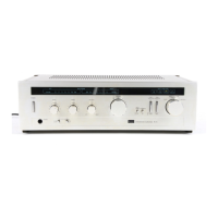
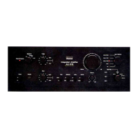
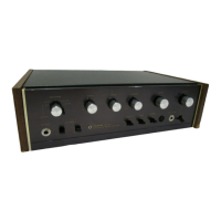
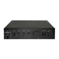
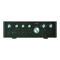
List of parts visible on the front panel.
List of parts visible on the top chassis.
Block diagram for the driver amplifier integrated circuit.
Block diagram for the speaker protector integrated circuit.
Block diagram for the quad analog switch integrated circuit.
Block diagram for the operational amplifier integrated circuit.
Block diagram for the operational amplifier integrated circuit.
List of materials used for packaging the unit.
List of accessories provided with the unit.
Complete circuit schematic showing all interconnected boards.