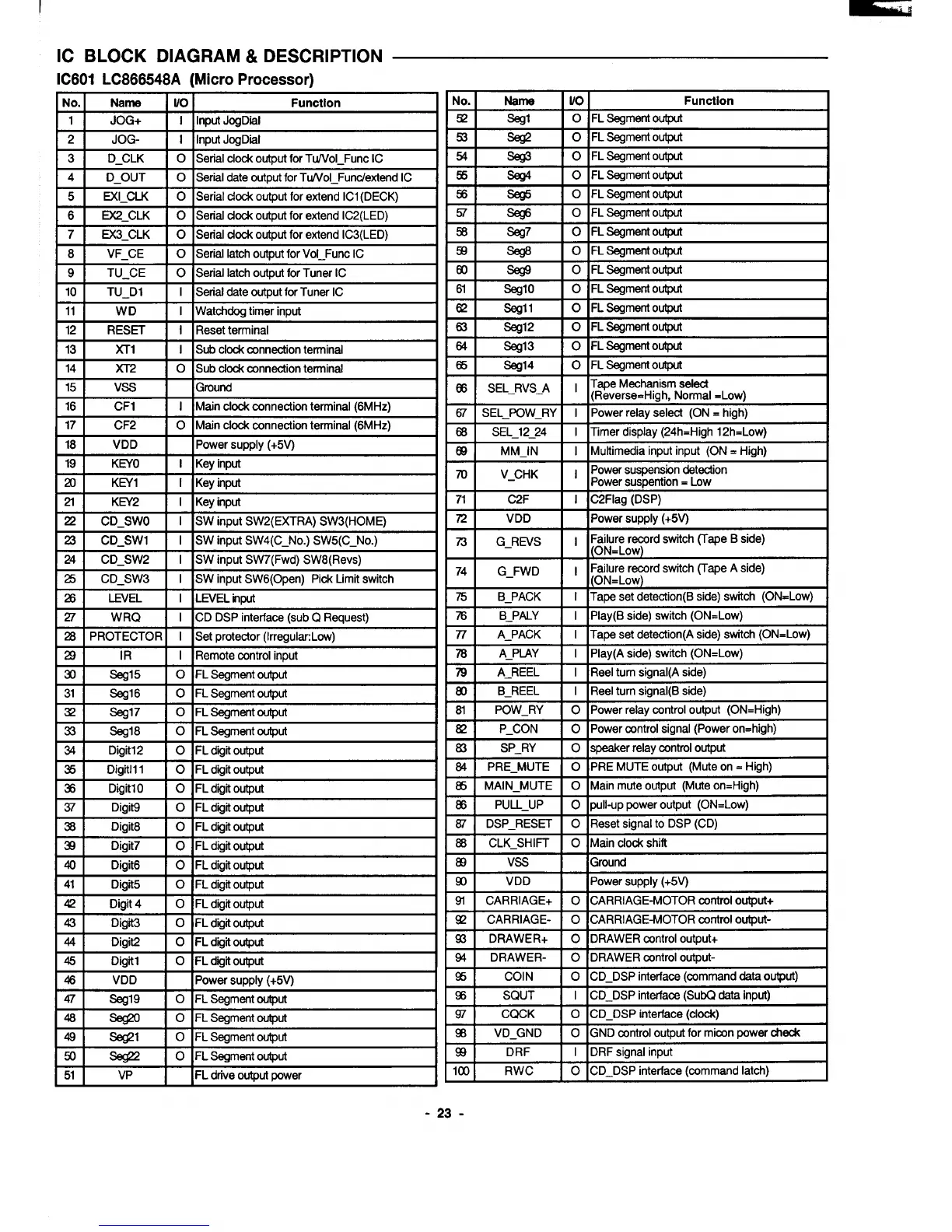
IC BLOCK DIAGRAM& DESCRIPTION —
IC601 LC866548A (Micro Processor)
No. Name Vo Function
S? Se@
o FL Segment output
53
0 FL segment ou@rt
54
0 FL Segment output
No. Nama
I/o
Function
1 JOG+ I Inpui JcgDHl
2
JOG-
1 Input JogDHl
3 D_CLK
o Serial clock output for TuArol_Func IC
4 D_OUT
o Serial date output for Tu/Vol_Func4extend IC
5
Exl_cLK o Serial deck output for extend ICI (DECK)
6
DC_CLK
o Serial dock outPut for extend IC2(LED)
55
0 FL Segment output
!3
o FL Segment output
5? o FL Segment output
58
seg7
o FL Segment output
59
0 FL Segment output
al
Se@
o FL Seament output
7 H3_cLK
o Serial dock output for extend IC3(LED)
8
VF_CE
o Serial latch output for Vol_Func IC
9
TU CE
o Serial latch outouf for Tuner IC
6t seg:o
o FL Segment output
@
S@ 1
0 FL Segment output
63 sea12
o FL Seoment outswt
t 1 1
10 I TU D1
I
I I.Serial date outDut for Tuner IC
I
—
11
WD I Watchdog timer input
12 RESET I Reset terminal
I I I
641
sea13
I
o IFL Seament oubut
I
13 Xrl I Sub clock connection terminal
14 X-r2
o Sub dock connection terminal
15 Vss Ground
16 CF1
I
Main clock connection terminal (6MHz)
17
CF2
o
Main clock connection terminal (6MHz)
1 1
1
61 se914 I 0 IFL segment output
I
68 SEL_RVS_A
, Tape Mechanism select
(Reverse=High, Normal =Low)
67 SEL_POW_RY I Power relay select (ON = high)
63 SEL_12_24
I Timer display (24h=High 12h=Low)
18 VDD Power supply (+5V)
19 KEYO I Key input
23 KEY1 I Key input
w
MM_lN I Multimedia input input (ON = High)
m
V_CHK
1 Power suspension detection
Power suspension = Low
71
C2F
I C2Flag (DSP)
I 2t I KEY2 ] I lKeyinput
I
z
CD_SWO
I SW input SW2(EXTRA) SW3(HOME)
23 CD_SWl
I SW input SW4(C_No.) SW5(C_N0.)
24 CD SW2
1
SW input SW7(Fwd) SW8(Revs)
721
VDD
I
IPower supply (+5V)
I
73
G_REVS
I
I
Failure record switch (Tape B side)
(C)N=I OW)
I
74
G_FWD
I
l(ON=LOw’~
1
Failure record switch (Tape A side)
751 B PACK I I lTaoe set detection(B side) switch (ON=LOW)
—
. . . .
25
CD_SW3
I SW input SW6(Open) Pick Limit switch
26
LEVEL I LEVEL input
1
—
1 t
.,
761 B PALY I lPlay(B side) switch (ON=LOW)
1
27 WRQ I CD DSP interface (sub Q Request)
a PROTECTOR I Set protector (lrregulacLow)
29 IR
I Remote control inDut
1
.
771
A_PACK I lTaw set detection(A side) switch (ON=LOW) I
I lPlay(A side) switch (ON=LOW)
I I Reel turn sirmal(A side)
1 1
1
331 %915
I
o IFL Segment output
I
1
—
I 1
-..
831
B_REEL
I
I lReel turn signal(B side)
I31
Se916
o FL Segment output
32 %917
o FL Segment output
33 Sa918 o FL Segment output
34
Digit12
o FL dgit
OU@Jf
?6
Digitll 1
0 FL dgit
OU@Jf
36
Digit10 o FL dgk O@X.Jt
37
Digit9
o FL dgit OUtpUf
38
Digit8
o FL dgi OIJ@Jt
39
Digit7 o FL digti OU@Ut
8f I POW_Rf o Power relay umtrol output (ON= High)
o Power control signal (Power on=high)
o speaker relay control outPut
1
—
64]
PRE_MUTE
,
0 IPRE MUTE output (Mute on. High)
I
=1=
85 MAIN_MUTE
83
Puu_uP
67
DSP_RESET
m CLK_SHIFT
-
0 Main mute output (Mute on. High)
Iml Vss I lGround
I
I 40 I Digit6 I O IFL digt output
I
E
(n VDD
91 CARRIAGE+
92
CARRIAGE-
93 DRAWER+
94
DRAWER-
95 COIN
96 SQUT
Power supply (+5~
o CARRIAGE-MOTOR control output+
o CARRIAGE-MOTOR control ouWt-
41 Digit5
0 FL digit
Ol@lf
42
Digit 4
0 FL dgit OUtfXlt
43
Diait3
o FL dmit OUtDUt
m
o I DRAWER control output+
I
1
1
1
-.
441 Digit2
I
o IFL dgit OUUM
I
, , ,
451 Digitl
I
o IFL dgit ouw
I
o DRAWER control output-
0 CD_DSP interface (command data output)
I CD_DSP interface (SubQ data input)
46
VDD Power supply (+5V)
47
%919 o FL Segment output
46 0 FL Segment output
49 Seg21 o FL Segment output
3+
!Z”
CQCK
96 VD_GND
99
DRF
la) RWC
o CD_DSP interface (dock)
o GND control output for mimn power check
I DRF signal inmd
50
0 FL Segment output
51 VP
FL drive output power
,
-.
0 lCD_DSP interface (command latch)
I
-23-
 Loading...