CD-MD3000H/CD-MD3000W
– 100 –
In this unit, the terminal with asterisk mark (*) is (open) terminal which is not connected to the outside.
(*): Normaly the output pin. Used as an I/O pin in test mode, which is not available to user applications.
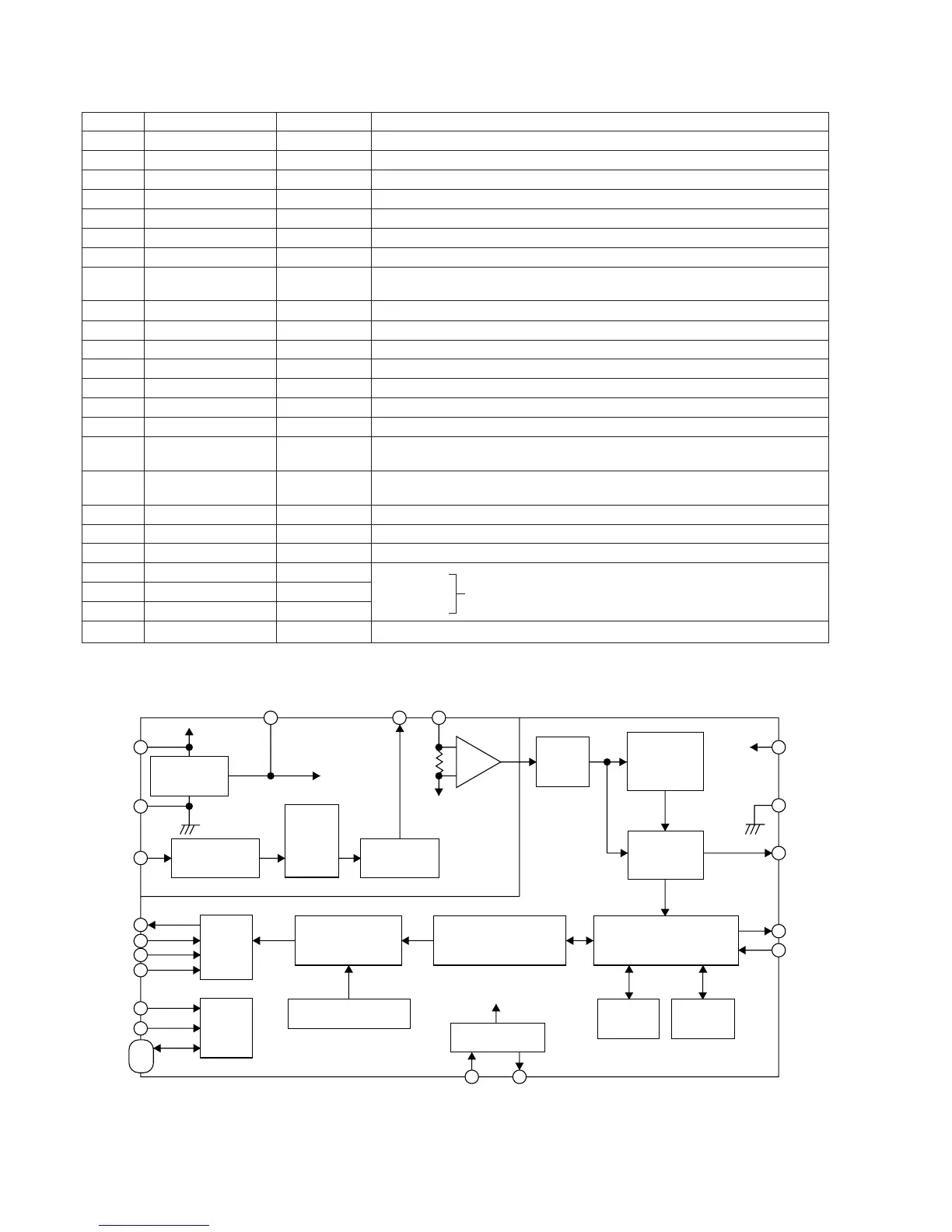
FunctionPort Name Input/Output
Pin No.
ICT21 VHiLC72722/-1: RDS Decorder (LC72722) (For CD-MD3000H Only)
1 VREF Output Reference voltage output (Vdda/2)
2 MPXIN Input Baseband (multiplexed0 signal input
3 VDDA — Analog power supply (+5V)
4 VSSA — Analog ground
5 FLOUT Output Subcarrier output (fulter output)
6 CIN Input Subcarrier input (comparator input)
7 T1 Input Test input (This pin must always be connected to ground.)
8 T2 Input Test input (standby control)
0: Normal operation 1: standby state (crystal oscillator stopped)
9* T3 (RDCL) Input/Output (*) Test I/O (RDS clock output)
10* T4 (RDDA) Input/Output (*) Test I/O (RDS data output)
11* T5 (RSFT) Input/Output (*) Test I/O (soft-decision control data output)
12 XOUT Output Crystal oscillator output (4.332/8.664 MHz)
13 XIN Input Crystal oscillator input (external reference signal input)
14 VDDD — Digital power supply (+5V)
15 VSSD — Digital ground
16* T6 Input/Output (*) Test I/O (error status, regenerated carrier, TP, error block count outputs)
(ERROR/57K/TP/BE1)
17* T7 Input/Output (*) Test I/O (error correction status, SK detection, TA, error block count outputs)
(CORREC/ARI-ID/TA/BE0)
18* SYNC Input/Output (*) Block synchronization detection output
19* RDS-ID Output RDS detection output
20 DO Output Data output
21 CL Input Clock input
22 DI Input Data input Serial data interface (CCB)
23 CE Input Chip enable
24 SYR Input Synchronization and RAM address reset (active high)
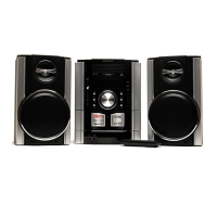
VREF FLOUT CIN
Vddd
Vssd
RDS-ID
SYNC
SYR
XOUT
XIN
DO
CL
DI
CE
T1
T2
T3 to T7
MPXIN
Vssa
Vdda
REFERENCE
VOLTAGE
ANTIALIASING
FILTER
57kHz
BPF
(SCF)
VREF
SMOOTHING
FILTER
+
_
PLL
(57kHz)
CLOCK
RECOVERY
(1187.5Hz)
DATA
DECODER
SYNC/EC CONTROLLER
SYNC
DETECT-2
SYNC
DETECT-1
ERROR CORRECTION
(SOFT DECISION)
CLK(4.332MHz)
OSC/DIVIDER
RAM
(24 BLOCK DATA)
MEMORY CONTROL
CCB
TEST
3
156
4
2
20
21
22
23
13 12
24
18
19
15
14
7
8
9~11,
16,17
Figure 100 BLOCK DIAGRAM OF IC