– 41 –
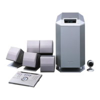
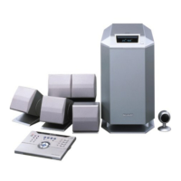
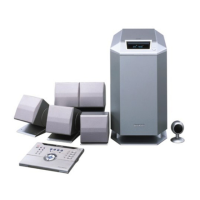
HT-CN300
IC710 RH-iX0489AWZZ: System Microcomputer (IX0489AW) (1/2)
1 P96/ANEX1/SOUT4 FLD_SDAT Output Display data output to M66005FP-FL driver.
2 P95/ANEX0/CLK4 FLD_SCK Output Serial clock output to M66005FP-FL driver.
3 P94/DA1/TB4IN FLD_CS Output CS control output to M66005FP-FL driver.
4 P93/DA0/TB3IN FLD_RESET Output Reset output to M66005FP-FL driver.
5* P92/TB2IN/SOUT3 DVD_KDATA Output Control data output to the DVD unit.
6 P91/TB1IN/SIN3 DVD_DATA Input DVD/CD/VCD data input from the DVD unit.
7* P90/TB0IN/CLK DVD_CLK Output Serial clock output to the DVD unit.
8 BYTE BYTE Input Connected to VSS due to unused external bus.
9 CNVSS FLASH_VCC Input
Used in the single chip mode. Connected to VSS via pull-down resistance.
10 P87/XCIN DVD_STB Input Strobe input from the DVD unit.
11* P86/XCOUT DVD_ERITE Output “L” - DVD microcomputer ROM write mode.
12 RESET RESET Input Microcomputer reset input. Active “L”.
13 XOUT X_OUT Output Microcomputer reference oscillation output.
14 VSS GND — Connected to GND (VSS).
15 XIN X_IN Input Microcomputer reference oscillation input
16 VCC VCC Input Microcomputer power supply (3.3 V)
17 P85/MNI FLASH_"H" Input Connected to VCC via pull-up resistance.
18 P84/INT2 SYS_STOP Input
Power failure detection input. Microcomputer enters the backup mode.
19 P83/INT1 GND — Port processing. “L” fixed.
20 P82/INT0 RX_IN Input Sharp method, remote control input..
21* P81/TA4IN/U TIMER_LED Output Timer stand-by LED control.
22 P80/TA40UT/U DD_LED Output Dolby digital IND.
23 P77/AT3IN STD_LED Output Surround mode stanrd IND.
24 P76/TA3OUT DTS_LED Output DTS IND.
25 P75/TA2IN/W VIR_LED Output Surround mode virtual IND.
26 P74/TA2OUT/W AAC_LED Output AAC IND.
27
P73/CTS2/RT2S/TA1IN/V
DPL_LED Output Dolby pro logic IND.
28 P72/CLK2/TA1OUT/V
F-CONT2
Input
Switches power supply frequency and changes oscillation frequency.
29
P71/RXD2/SCL/TA0IN/TB5IN
SCL Output AK4586/CXA2125Q. 12C BUS clock output.
30
P70/TXD2/SDA/TA0OUT
SDA Input/Output AK4586/CXA2125Q. 12C BUS data input/output.
31 P67/TXD1 FLASH_TXD Output Functionally not used. Normally, output “L” fixed.
32 P66/RXD1 FLASH_RXD Output Functionally not used. Normally, output “L” fixed.
33 P65/CLK1 FLASH_SLOCK Output Functionally not used. Normally, output “L” fixed.
34
P64/CTS1/RTS1/CTS0/CLKS1
FLASH_BUSY Output Functionally not used. Normally, output “L” fixed.
35 P63/TXD0 DSP_SCDIN Output DSP IC serial data output.
36 P62/RXD0 DSP_SCDOUT Input DSP IC serial data output.
37 P61/CLK0 DSP_SCCLK Output Sends DSP IC serial send/receive sync clock.
38 P60/CTS0/RTS0 DSP_CS Input Sends DSP IC serial send/receive strobe.
39 P57/RDY/CLKOUT DSP_RESET Output DSP IC RESET output.
40* P56/ALE L-MUTE Output VCR OUT audio mute output.
41 P55/HOLD FLASH_EPM Input Connected to VSS via pull-down resistance.
42 P54/HLDA AUDITION Input Audition model select input.
43* P53/BCLK F_CONT Output
Switches power supply frequency and changes oscillation frequency.
44* P52/RD FM_STB Output
When function is set to “FM Stereo” or “FM MONO”: “L”. Otherwise: “H”.
45 P51/WRH/BHE DSP_UC15 Output External ROM for DSP download program.
46 P50/WRL/WR FLASH_CE Input Connected to VCC via pull-up resistance.
47 P47/CS3 DSP_UC16 Output External ROM for DSP download program.
48 P46/CS2 DSP_UC17 Output External ROM for DSP download program.
49 P45/CS1 ASPECT Input DVD unit aspect ratio data input.
50 P44/CS0 V-MODE Input Video mode select SW input terminal.
51* P43/A19 V_SEL1 Output Connected to video output selector, SW1.
Port Name
Terminal Name
Pin No.
Input/Output
Function
In this unit, the terminal with asterisk mark (*) is (open) terminal which is not connected to the outside.