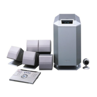
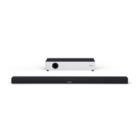
HT-CN410DVH
64
IC251, VFD Driver (PT6311)
Pin Description:
Pin Name I/O Function Pin No.
SW1 to SW4 I General Purpose Input pins 1 to 4
DOUT O
Data Output Pin (N-Channel, Open-Drain)
This pin outputs serial data at the falling edge of the shift clock (starting from the
lower bit)
5
DIN I
Data Input Pin
This pin inputs serial data at the rising edge of the shift clock
(starting from the lower bit)
6
NC - No Connection 7
CLK I
Clock Input pin
This pin reads serial data at the rising edge and
outputs data at the falling edge.
8
STB I
Serial Interface Strobe pin
The data input after the STB has fallen is
processed as a command.
When this pin is “HIGH”, CLK is ignored.
9
K1 to K4 I
Key Data Input Pins
The data inputted to these pins are latched at
the end of the display cycle.
10 to 13
VDD - Logic Power Supply 14, 33, 45
SG1/KS1 to SG12/KS12 O
High-Voltage Segment Output Pins
Also acts as the Key Source
15 to 26
SG20/GR9 to SG19/GR10
SG18/GR11 to SG13/GR16
O High Voltage Segment / Grid Output Pins
36 to 35
32 to 27
VEE - Pull-Down Level 34
GR1 to GR8 O High- Voltage Grid Output Pins 44 to 37
LED1 to LED5 O LED Output Pin 50 to 46
GND - Ground Pin 51
OSC I
Oscillator Input Pin
A resistor is connected to this pin to determine
the oscillation frequency
52