104
LC-26GA5E
LC-32GA5E
LC-26GA5E
LC-32GA5E
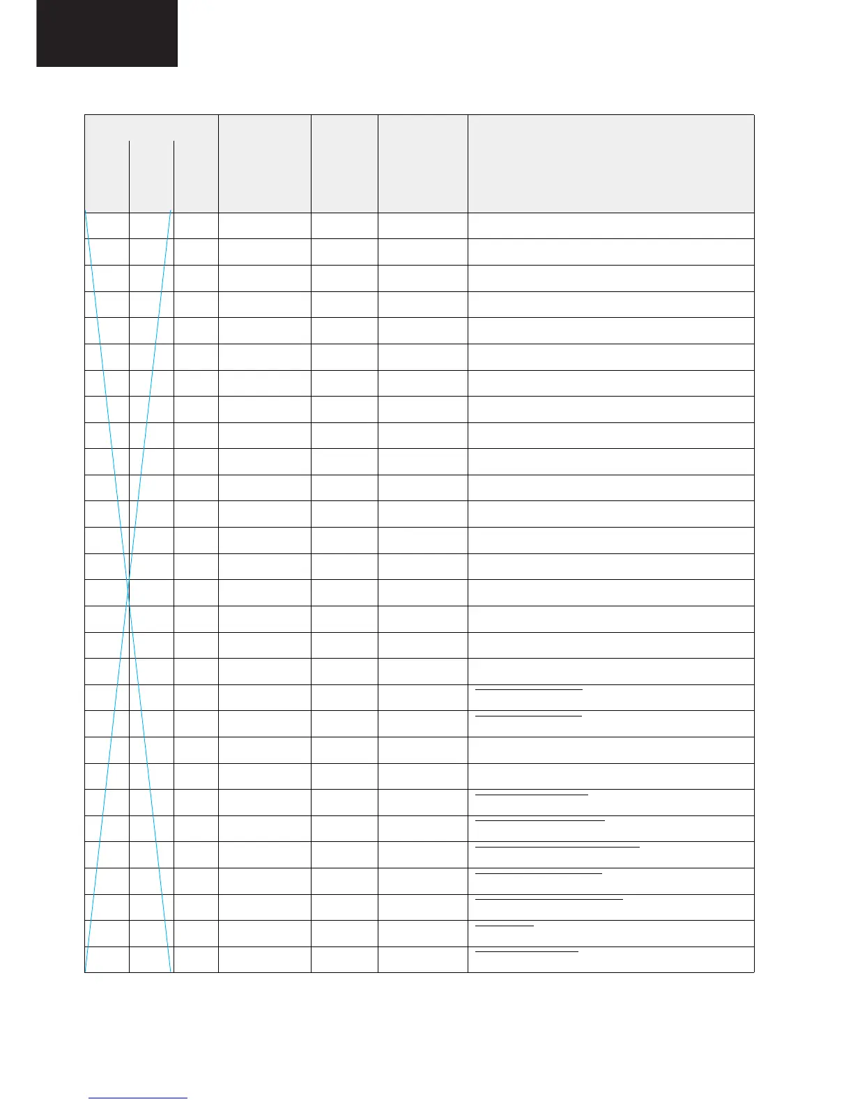
1.3. Description of Pins IC1001, continued
15 ADB9 OUT LV Address Bus 9 Output
16 ADB8 OUT LV Address Bus 8 Output
27 ADB7 OUT LV Address Bus 7 Output
28 ADB6 OUT LV Address Bus 6 Output
29 ADB5 OUT LV Address Bus 5 Output
30 ADB4 OUT LV Address Bus 4 Output
84 ADB3 OUT LV Address Bus 3 Output
85 ADB2 OUT LV Address Bus 2 Output
86 ADB1 OUT LV Address Bus 1 Output
87 ADB0 OUT LV Address Bus 0 Output
88 DB0 IN/OUT LV Data Bus 0 Input/Output
89 DB1 IN/OUT LV Data Bus 1 Input/Output
90 DB2 IN/OUT LV Data Bus 2 Input/Output
91 DB3 IN/OUT LV Data Bus 3 Input/Output
92 DB4 IN/OUT LV Data Bus 4 Input/Output
93 DB5 IN/OUT LV Data Bus 5 Input/Output
94 DB6 IN/OUT LV Data Bus 6 Input/Output
95 DB7 IN/OUT LV Data Bus 7 Input/Output
32 RDQ OUT LV Data Read Enable
Output
33 WRQ OUT LV Data Write Enable
Output
34 OCF OUT LV Opcode Fetch Output
35 ALE OUT LV Address Latch Enable Output
36 RSTQ OUT LV Internal CPU Reset
Output
97 PSENQ OUT LV Program Store Enable
Output
20 PSWEQ OUT LV Program Store Write Enable
Output
51 XROMQ IN OBL External ROM Enable
Input
52 EXTIFQ IN LV Enable External Interface
Input
24 STOPQ IN LV Stop CPU
Input
25 ENEQ IN LV Enable Emulation
Input
Pin No. Pin Name Type Connection
(If not used)
Short Description
PSSDIP88-1
PY
PSSDIP88-1
PZ
PMQFP144-2
XM