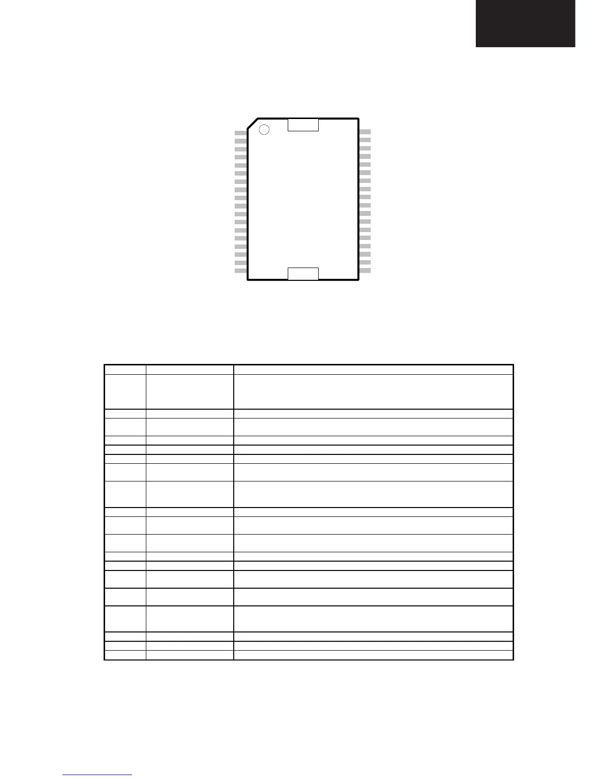
Pin Function Description
2, 3 DCAP2, DCAP1 Charge pump switching pins. DCAP1 (pin 3) is a free running 300kHz square
wave between VDDA and DGND (12Vpp nominal). DCAP2 (pin 2) is level shifted
10 volts above DCAP1 (pin 3) with the same amplitude (12Vpp nominal),
frequency, and phase as DCAP1.
4, 9 V5D, V5A Digital 5VDC, Analog 5VDC
5, 8,
17
AGND1, AGND2,
AGND3
Analog Ground
6 REF Internal reference voltage; approximately 1.0 VDC.
7 OVERLOADB A logic low output indicates the input signal has overloaded the amplifier.
10, 14 OAOUT1, OAOUT2 Input stage output pins.
11, 15 INV1, INV2 Single-ended inputs. Inputs are a “virtual” ground of an inverting opamp with
approximately 2.4VDC bias.
12 MUTE When set to logic high, both amplifiers are muted and in idle mode. When low
(grounded), both amplifiers are fully operational. If left floating, the device stays in
the mute mode. This pin should be tied to GND if not used.
16 BIASCAP Input stage bias voltage (approximately 2.4VDC).
18 SLEEP When set to logic high, device goes into low power mode. If not used, this pin
should be grounded
19 FAULT A logic high output indicates thermal overload, or an output is shorted to ground,
or another output.
20, 35 PGND2, PGND1 Power Grounds (high current)
22 DGND Digital Ground. Connect to AGND locally (near the TA2024).
24, 27;
31, 28
OUTP2 & OUTM2;
OUTP1 & OUTM1
Bridged output pairs
25, 26,
29, 30
VDD2, VDD2
VDD1, VDD1
Supply pins for high current H-bridges, nominally 12VDC.
13, 21,
23, 32,
34
NC Not connected. Not bonded internally.
33 VDDA Analog 12VDC
36 CPUMP Charge pump output (nominally 10V above VDDA)
1 5VGEN Regulated 5VDC source used to supply power to the input section (pins 4 and 9).