LC-26SA1E/RU, LC-32SA1E/RU
7 – 18
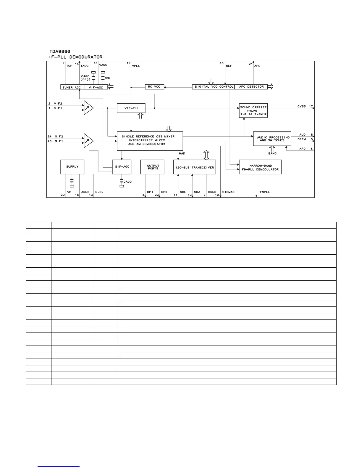
2.8. IC201 (VHITDA9886+-1Y)
2.8.1 Block Diagram
2.8.2 Pin Connections and short description
Pin No. Pin Name I/O Pin Function
1 VIF1 I VIF differential input 1
2 VIF2 I VIF differential input 2
3 OP1 O Output port 1; open-collector.
4 FMPLL I FM-PLL for loop filter.
5 DEEM O De-emphasis output for capacitor.
6 AFD I AF decoupling input for capacitor
7 DGND – Digital ground.
8 AUD O Audio output.
9 TOP I Tuner AGC TakeOver Pint (TOP) for resistor adjustment.
10 SDA I/O I2C-bus data input and output.
11 SCL I I2C-bus clock input.
12 SIOMAD O Sound intercarrier output and MAD select with resistor.
13 N.C. – Not connected.
14 TAGC O Tuner AGC output.
15 REF I 4 MHz crystal or reference signal input.
16 VAGC(1) I VIF-AGC for capacitor.
17 CVBS O Composite video output.
18 AGND – Analog ground.
19 VPLL I VIF-PLL for loop filter.
20 VP – Supply voltage.
21 AFC O AFC output.
22 OP2 O Output port 2; open-collector.
23 SIF1 I SIF differential input 1 and MAD select with resistor.
24 SIF2 I SIF differential input 2 and MAD select with resistor.