9397 750 13847 © Koninklijke Philips Electronics N.V. 2005. All rights reserved.
Preliminary data sheet Rev. 01 — 14 January 2004 3 of 31
Philips Semiconductors
TDA8931
Power comparator 1 × 20 W
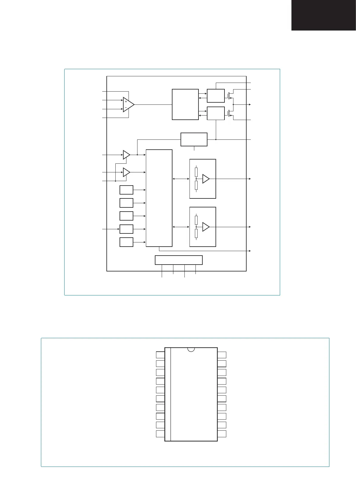
6. Block diagram
Fig 1. Block diagram
001aab807
TDA8931
UVP
HEAT SPREADER
CONTROL
comparator
CONTROL
DRIVER
HIGH
STABILIZER
12V
BOOT
V
DDP
17
18
OUT
16
V
SSP
15
STABI
V
SSD
V
DDP
V
SSP
14
HVP
13
V
DDP
V
SSP
HVPI
19
DIAG
8
12
1 10 11 20
V
SSD
V
SSD
V
SSD
V
SSD
DRIVER
LOW
OVP
OVP
9
CGND
7
ENABLE
6
POWERUP
3
INN
4
INP
OCP
OTP
2
V
SSA
5
V
DDA
ODP
9397 750 13847 © Koninklijke Philips Electronics N.V. 2005. All rights reserved.
Preliminary data sheet Rev. 01 — 14 January 2004 4 of 31
Philips Semiconductors
TDA8931
Power comparator 1 × 20 W
7. Pinning information
7.1 Pinning
7.2 Pin description
Fig 2. Pin configuration
TDA8931
V
SSD
V
SSD
V
SSA
HVPI
INN V
DDP
INP BOOT
V
DDA
OUT
POWERUP V
SSP
ENABLE STABI
DIAG HVP
CGND OVP
V
SSD
V
SSD
001aab811
1
2
3
4
5
6
7
8
9
10
12
11
14
13
16
15
18
17
20
19
Table 3: Pin description
Symbol
Pin
Description
V
SSD
1 negative digital supply voltage; heat spreader
V
SSA
2 negative analog supply voltage
INN 3 inverting input
INP 4 non inverting input
V
DDA
5 positive analog supply voltage
POWERUP 6 power-up input
ENABLE 7 enable input
DIAG 8 diagnostic output
CGND 9 control ground; reference ground for pins POWERUP, ENABLE and DIAG
V
SSD
10 negative digital supply voltage; heat spreader
V
SSD
11 negative digital supply voltage; heat spreader
OVP 12 overvoltage protection reference input
HVP 13 half supply voltage output for charging SE capacitor
STABI 14 decoupling of internal stabilizer
V
SSP
15 negative power supply voltage
OUT 16 PWM output
BOOT 17 bootstrap capacitor connection
V
DDP
18 positive power supply voltage
HVPI 19 half supply voltage output for reference voltage of input circuitry
V
SSD
20 negative digital supply voltage; heat spreader