7283434C STMicroelectronics Confidential 7/66
STV0360 Pin information
Confidential
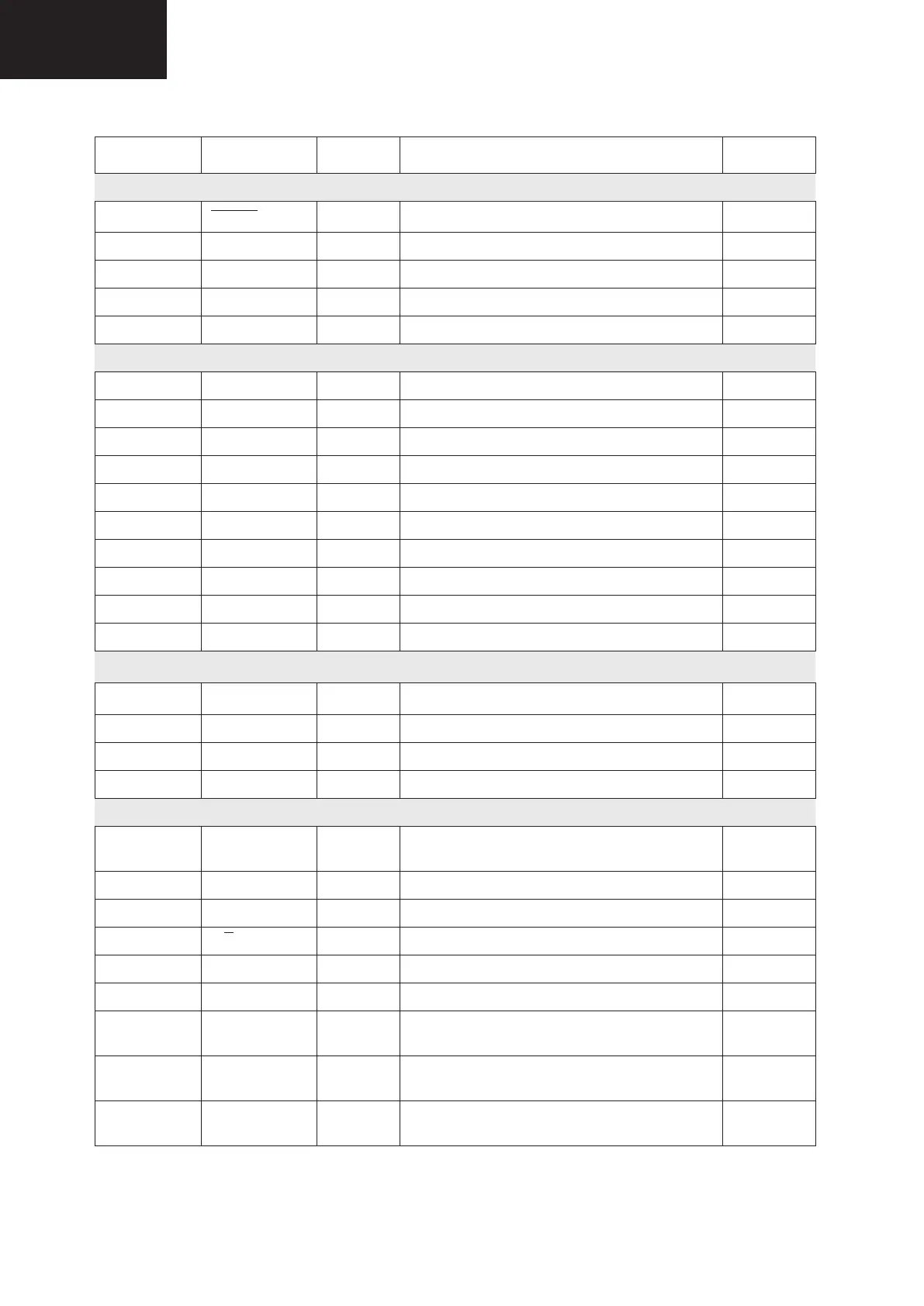
3.2 Pinout description (preliminary)
Table 1: STV0360 pin description
Pin number Name Type Description Drive (mA)
Clock and resets
12 RESET I
1
Hardware reset, active low -
62 XTALI Analog Crystal oscillator input/external clock (1.8 V) -
63 XTALO Analog Crystal oscillator output -
61 VCCXTAL1.8 Supply Analog oscillator supply (1.8 V) -
64 GNDXTAL Ground Analog oscillator ground -
Analog interface
2 DVCCA1.8 Supply Analog part digital supply (1.8 V) -
5 REFM Analog Internal negative reference -
6 REFP Analog Internal positive reference
3 VCCA1.8 Supply Analog supply (1.8 V) -
9 INM Analog Negative analog input -
10 INP Analog Positive analog input -
4, 11 GNDA Supply Analog ground -
1 DGNDA Ground Analog ground -
7 VR Analog Reference -
8 VCCA3.3 Supply Analog supply (3.3 V)
I
2
C interface
21 SDA IO
2
Serial data (open drain) 8
20 SCL I Serial clock (open drain) -
19 SDAT IO SDA tuner (open drain) 4
18 SCLT I SCL tuner
MPEG interface
25, 26, 27, 29,
31, 32, 33, 34
D7/0
O
3
Serial D7, MPEG data 8/4
36 CLK_OUT O MPEG byte or bit clock 4
23 STR_OUT O MPEG first byte sync 2
38 D/P
O MPEG data valid/parity 4
40 ERROR O MPEG packet error 2
51 HFEC0 O Hierarchical FEC output bit 0 2
50 CCLK/HFEC1 O Hierarchical FEC output bit 1 or clock for
constellation display
2
49 CDATA/HFEC2 O Hierarchical FEC output bit 2 or data for
constellation display
2
48 CIQ/HFEC3 O Hierarchical FEC output bit 3 or IQ validation for
constellation display
2