LC-37XD1E/RU
5 – 16
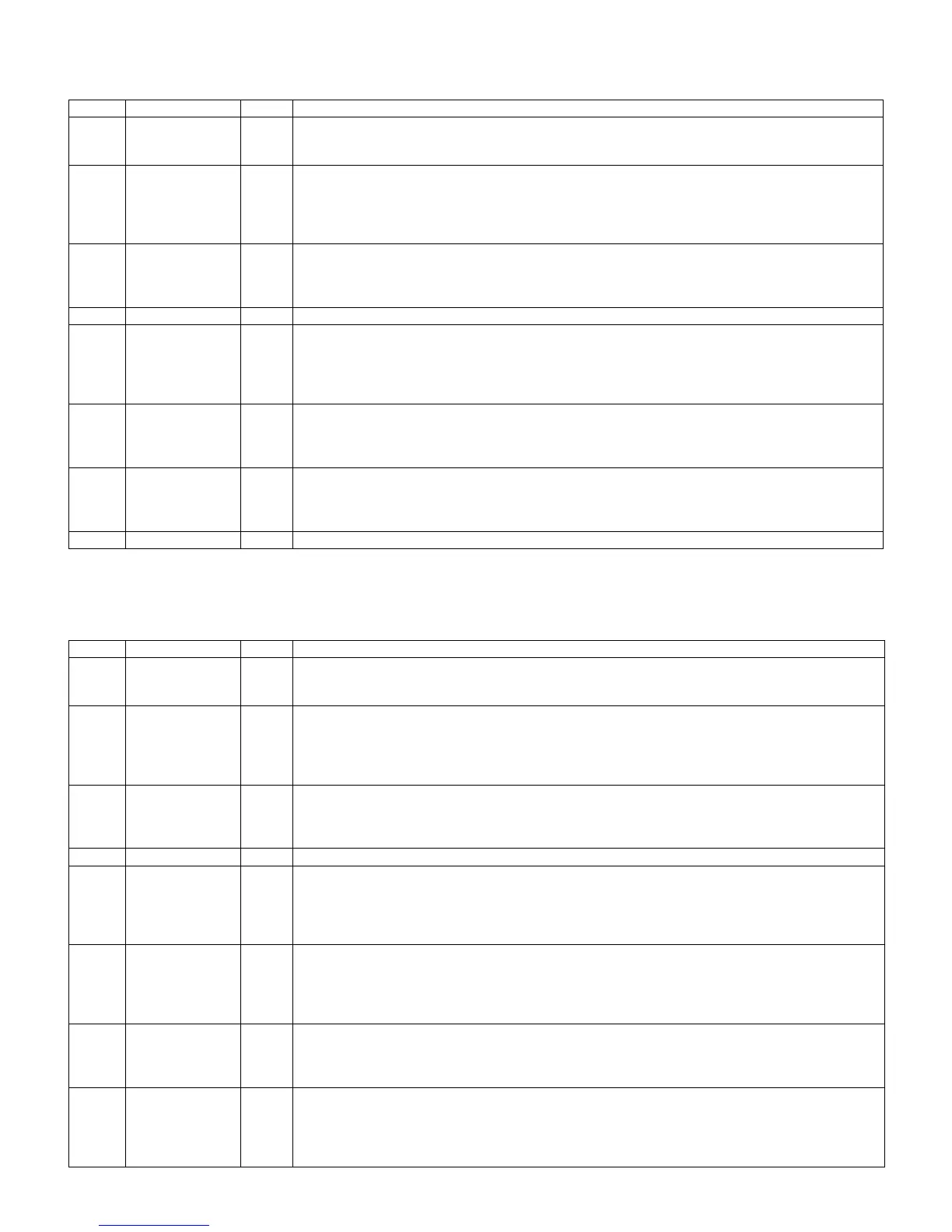
9. IC1712: VHIMP1410ES-1
Step Down Converter.
10. IC1706: VHIMP1583++-1
Step Down Converter
Pin No. Pin Name I/O Pin Function
1 BS I High-Side Gate Drive Boost input.
BS supplies the drive for the high-side n-channel MOSFET switch.
Connect a 10nF or greater capacitor from SW to BS to power the high-side switch.
2 IN I Power input.
IN supplies the power to the IC,as well as the step-down converter switches.
Drive IN with a 4.75V to 15V power source.
Bypass IN to GND with a suitably large capacitor to eliminate noise on the input to the IC.
See input Capacitor.
3 SW O Power Switching Output.
SW is the switching node that supplies power to the output.
Connect the output LC filter from SW to the output load.
Note that a capacitor is required from SW to BS to power the high-side switch.
4 GND - Ground.
5 FB I Feedback input.
FB senses the output voltage to regulate that voltage.
Drive FB with a resistive voltage divider from the output voltage.
The feedback threshold is 1.22V.
See Setting the Output Voltage.
6 COMP - Compensation Node.
COMP is used to compensate the regulation control loop.
Connect a series RC network from COMP to GND to compensate the regulation control loop.
See Compensation.
7 EN I Enable input.
EN is a digital input that turns the regulator on or off.
Drive EN high to turn on the regulator,drive it low to turn it off.
For automatic startup,leave EN unconnected.
8 N/C - No Connect.
Pin No. Pin Name I/O Pin Function
1 BS I High-Side Gate Drive Boost lnput.
BS supplies the drive for the high-side n-channel MOSFET Switch.
Connect a 4.7nF or greater capacitor from SW to BS to power the high side switch.
2 IN I Power input.
IN supplies the power to the IC, as well as the step-down converter switches.
Drive IN with a 4.75V to 23V power source.
Bypass IN to GND with a suitably large capacitor to eliminate noise on the input to the IC.
See Input Capacitor.
3 SW O Power Switching Output.
SW is the switching node that supplies power to the output.
Connect the output LC filter from SW to the output load.
Note that a capacitor is required from SW to BS to power the high-side switch.
4 GND - Ground. (Note: Connect the exposed pad on backside to Pin4).
5 FB I Feedback input.
FB senses the output voltage to regulate that voltage.
Drive FB with a resistive voltage divider from the output voltage.
The feedback threshold is 1.222V.
See Setting the Output Voltage.
6 COMP I Compensation Node.
COMP is used to compensate the regulation control loop.
Connect a series RC network from COMP to GND to compensate the regulation control loop.
In same cases, an additional capacitor from COMP to GND is required.
See Compensation.
7 EN I Enable input
EN is a digital input that turns the regulator on or off.
Drive EN high to turn on the regulator, drive it low to tum it off .
For automatic startup, leave EN unconnected.
8 SS I Soft Start Control input.
SS controls the soft start period.
Connect a capacitor from SS to GND to set the soft-start period.
A 0.1µF capacitor sets the soft-start period to l0ms
To disable the soft-start featur CIeave SS unconnected.