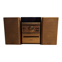
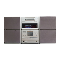
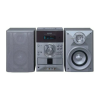
XL-MP333H/XL-MP444H
8 – 2
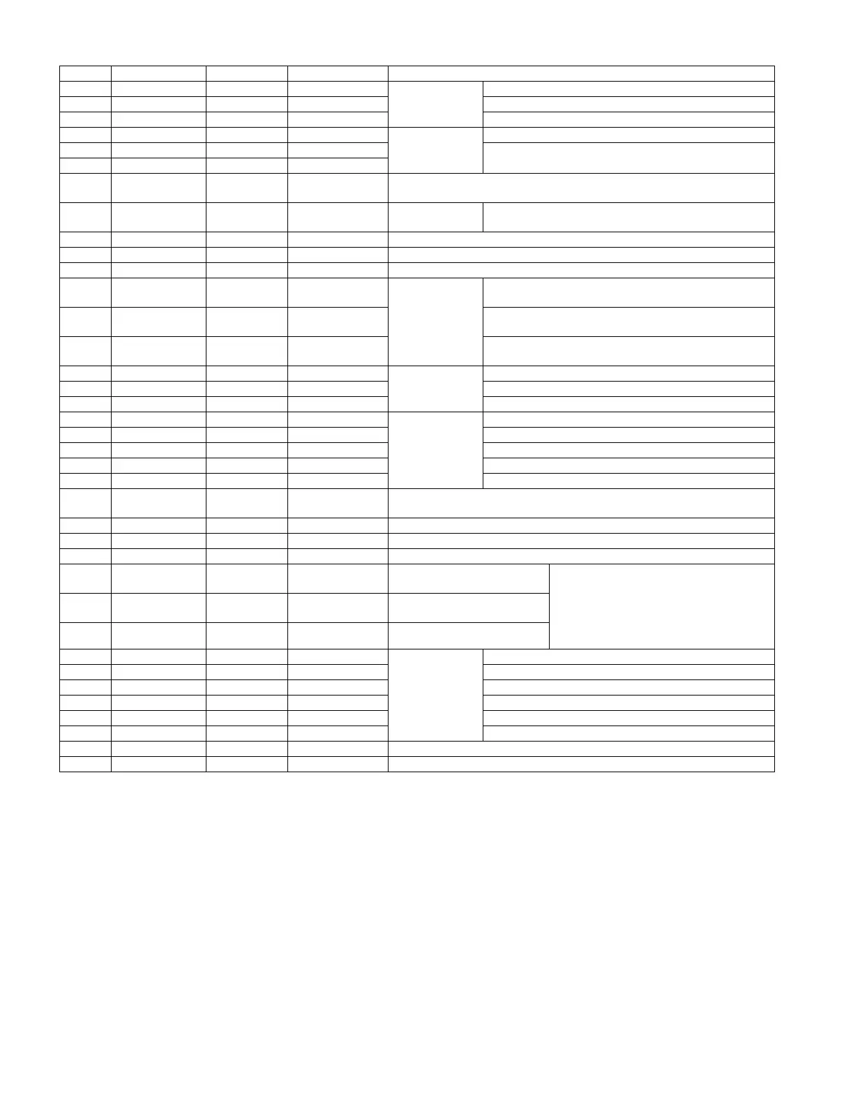
IC401 VHiLC78646E-1: CD Servo (LC78646E) (2/2)
In this unit, the terminal with asterisk mark (*) is (open) terminal which is not connected to the outside.
Be sure to supply the same potential to each power terminal. (VVDD, ADAVDD, VDD, LVDD, RVDD, XVDD)
Terminal witch is controlled by the power terminal (VDD5 V) for a microcomputer interface:
CE (61 pin), CL (62 pin), DI (63 pin), DO (64 pin), WRQ (65 pin), RES (66 pin), DRF (67 pin)
Pin No. Terminal Name Input/Output Setting in Reset Function
44 RVSS — —
Right channel
D/A converter
GND for Right channel. Must be connected to 0 V.
45 RCHO Output LVDD/2 Right channel output.
46 RVDD Input — Power supply for Right channel.
47 XVDD Input —
Crystal
Oscillator
Power supply for crystal oscillator.
48 XOUT Output Oscillator Connected for the 33.8688 MHz crystal oscillator cie-
ment.
49 XIN Input Oscillator
50 FSX/16MIN Input/Output Input 7.35 kHz Synchronization signal monitor port.
or Clock input port for Digital filter & D/A
51 XVSS — — Crystal
Oscillator
GND for crystal oscillator. Must be connected to 0 V.
52 C2F Output H C2 FLAG monitor port.
53* EFLG Output L C1, C2 error corrected monitor port.
54 16MOUT Output Clock 16.9344 MHz output port.
55 ASLRCK Input —
Anti-shock
Left/Right clock input port.
(If this port does not use, must be connect to 0 V.)
56 ASDACK Input — Bit clock input port.
(If this port does not use, must be connect to 0 V.)
57 ASDFIN Input — Left/Right channel data input port.
(If this port does not use, must be connect to 0 V.)
58 LRCK Output L
Digital data.
Left/Right clock output port.
59 DATACK Output L Bit clock output port.
60 DATA Output L Left/Right channel data output port.
61 CE Input —
Microcomputer
Interface
Chip enable signal input port.
62 CL Input — Data transfer clock input port.
63 DI Input — Data input port.
64 DO Output (H) Data output port. (N-ch. open drain output.)
65 *WRQ Output H Interruption signal output.
66 *RES Input — Chip reset signal input port.
This port must be set LOW after first applied power on.
67 DRF Output L Focus detection output port.
68 VDD5 Input — Power supply for Microprocessor.
69 VSS — — GND for digital circuit. Must be connected to 0 V.
70 CONT3 Input/Output Input General purpose port 3. Controlled with serial data command from
microcomputer. When not used, General
purpose input/output terminal. Set it as the
input terminal and open it by connecting to
0 V, or set it as the output terminal and
open it.
71* CONT2 Input/Output Input General purpose port 2.
72* CONT1 Input/Output Input General purpose port 1.
73 PDO1 Output —
PLL
Internal VCO control phase comparator output port 1.
74 PDO2 Output Input Internal VCO control phase comparator output port 2.
75 VVSS — — GND for internal VCO. Must be connected to 0 V.
76 PCKIST Input — PDO output current adjustment resistor connection port.
77 VVDD Input — Power supply for internal VCO.
78 FR Input — VCO frequency range adjustment port.
79 LDS Input — LASER power detected signal input port.
80 LDD Output — LASER power control signal output port.
 Loading...