7SR242 Duobias Description Of Operation
©2010 Siemens Protection Devices Limited Chapter 1 Page 3 of 52
5.4 OverFluxing Detector (81HBL5)..............................................................................................46
5.5 Demand...................................................................................................................................47
Section 6: Other Features....................................................................................................................48
6.1 Data Communications.............................................................................................................48
6.2 Maintenance............................................................................................................................48
6.2.1 Output Matrix Test......................................................................................................48
6.2.2 CB Counters...............................................................................................................48
6.2.3 I
2
t CB Wear ................................................................................................................48
6.3 Data Storage...........................................................................................................................49
6.3.1 General.......................................................................................................................49
6.3.2 Event Records............................................................................................................49
6.3.3 Waveform Records. ...................................................................................................49
6.3.4 Fault Records.............................................................................................................50
6.3.5 Demand/Data Log ......................................................................................................50
6.4 Metering ..................................................................................................................................50
6.5 Operating Mode ......................................................................................................................51
6.6 Control Mode...........................................................................................................................51
6.7 Real Time Clock......................................................................................................................51
6.7.1 Time Synchronisation – Data Comms .......................................................................52
6.7.2 Time Synchronisation – Binary Input .........................................................................52
6.7.3 Time Synchronisation – IRIG-B (Optional).................................................................52
6.8 Settings Groups ......................................................................................................................52
6.9 Password Feature...................................................................................................................52
List of Figures
Figure 1-1 Functional Diagram: 7SR242n-2aAnn-0AA0 Relay.............................................................9
Figure 1-2 Functional Diagram: 7SR242n-2aAnn-0BA0 Relay...........................................................10
Figure 1-3 Functional Diagram: 7SR242n-2aAnn-0CA0 Relay ..........................................................11
Figure 1-4 Connection Diagram: 7SR242 Relay.................................................................................12
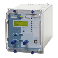
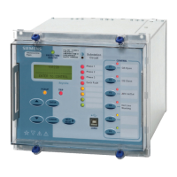
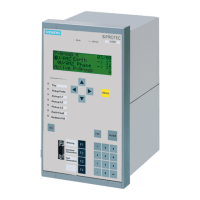
Figure 2-1 7SR24 with 3 + 16 LEDs in E8 Case................................................................................14
Figure 2-2 Binary Input Logic .............................................................................................................17
Figure 2-3 Binary Output Logic ..........................................................................................................19
Figure 3-1 Biased Differential Characteristic.......................................................................................21
Figure 3-2 Functional Diagram for Biased Current Differential Protection..........................................22
Figure 3-3 Differential Highset Characteristic .....................................................................................23
Figure 3-4 Logic Diagram: High Set Current Differential Protection ...................................................24
Figure 3-5 Logic Diagram: Instantaneous Over-current Element .......................................................25
Figure 3-6 Logic Diagram: Time Delayed Overcurrent Element .........................................................26
Figure 3-7 Logic Diagram: Instantaneous Derived Earth Fault Element ............................................27
Figure 3-8 Logic Diagram: Derived Time Delayed Earth Fault Protection..........................................28
Figure 3-9 Logic Diagram: Measured Instantaneous Earth-fault Element..........................................29
Figure 3-10 Logic Diagram: Time Delayed Measured Earth Fault Element (51G) ...............................30
Figure 3-11 Logic Diagram: High Impedance REF (64H) .....................................................................31
Figure 3-12 Logic Diagram: Open Circuit Function (46BC) ..................................................................32
Figure 3-13 Logic Diagram: Negative Phase Sequence Overcurrent (46NPS)....................................33
Figure 3-14 Logic Diagram: Undercurrent Detector (37, 37G)..............................................................34
Figure 3-15 Logic Diagram: Thermal Overload Protection (49) ............................................................36
Figure 3-16 Inverse Over-fluxing Characteristic (24IT) .........................................................................37
Figure 3-17 Logic Diagram: Overfluxing Elements (24)........................................................................38
Figure 3-18 Logic Diagram: Under/Over Voltage Elements (27/59) .....................................................39
Figure 3-19 Logic Diagram: Neutral Overvoltage Element ...................................................................40
Figure 3-20 Logic Diagram: Under/Over Frequency Detector (81).......................................................41
Figure 4-1 Sequence Diagram showing PU/DO Timers in Quick Logic (Counter Reset
Mode Off) ...........................................................................................................................43
Figure 5-1 Logic Diagram: Circuit Breaker Fail Protection (50BF)......................................................44
 Loading...