Smart Machine Smart Decision
SIM800L(MT6261)_Hardware Design_V1.01 50 2016-07-07
5. PCB Layout
Usually, most electronic products with good performance are based on good PCB layout. A bad PCB layout will
lead to lots of issues, like TDD noise, SIM card not be detected, etc. the final solution for these problems is to
redo PCB layout. Making good PCB layout at beginning will save develop schedule and cost as well.
This section will give some guidelines on PCB layout, in order to eliminate interfere or noise by greatest degree,
and save product development period.
5.1 Pin Assignment
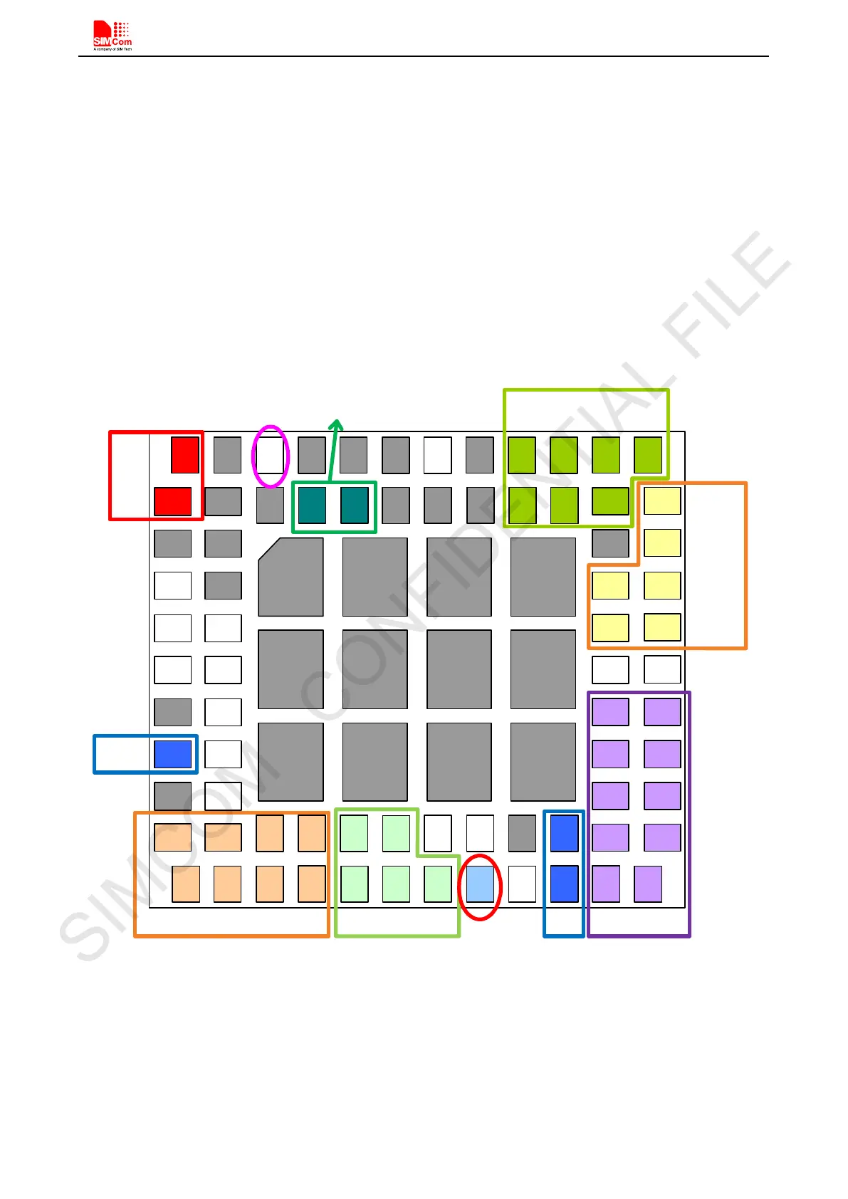
Before PCB layout, we should learn well about pin assignment in order to get reasonable layout with so many
external components. Following figure is the overview of pin assignment of the module.
GND
GND
GND
USB_DP
GND
GND
GND
GND
GND
GND
GND
GNDGND
GND
GNDGND
GND
GND
GND
VBAT
VBUS
Audio
SIM
FM
antenna
USB
KEY
PCM
UART
GSM
Antenna
I2C
GND
GND
GND
GND
GND
GNDGND
GND
GND GND
GND
Figure 50: Pin assignment
5.2 Principle of PCB Layout
During layout, attention should be paid to the following interfaces, like Antenna, power supply, SIM card