Do you have a question about the SONIX SN8P2511 and is the answer not in the manual?
Lists the main features and specifications of the SN8P2511.
Visualizes the internal structure and components of the microcontroller.
Details the pinout for different package types (P-DIP, SOP, SSOP).
Describes the function, type, and control conditions for each pin.
Shows typical circuit configurations for various pin types.
Describes the ROM layout including reset, interrupt, and general purpose areas.
Describes the 48-byte general purpose RAM and system registers.
Explains immediate, direct, and indirect addressing modes.
Explains how the stack pointer and buffer manage program flow.
Lists various code options affecting hardware configuration.
Summarizes the three main reset conditions and their impact.
Explains the sequence of events during a power-on reset.
Describes how the watchdog timer prevents system hangs.
Details the brown-out reset condition due to voltage drops.
Explains system operating voltage and its relation to reset voltage.
Describes the LVD feature for detecting low voltage conditions.
Introduces the dual clock system (high-speed and low-speed).
Explains Fcpu as the instruction cycle and its relation to clock sources.
Describes the Noise Filter's role in reducing high-frequency noise.
Details internal and external high-speed clock options.
Introduces the four operating modes: Normal, Slow, Power Down, Green.
Describes the Normal Mode, its clock source, and characteristics.
Explains Slow Mode using the internal low-speed RC oscillator.
Details the Power Down Mode for minimal power consumption.
Describes Green Mode for reduced power consumption with clock running.
Introduces the interrupt sources and control mechanisms.
Explains the INTEN register for enabling interrupt sources.
Describes the INTRQ register for tracking interrupt requests.
Explains the GIE bit for enabling/disabling all interrupts.
Details PUSH/POP instructions for saving register context during interrupts.
Describes the INTO external interrupt and its wake-up function.
Explains Timer 0 interrupt operation and its setup.
Details TC0 timer interrupt operation and its request flag.
Explains how to manage multiple interrupt requests and priorities.
Introduces the microcontroller's 12 I/O pins and their shared functions.
Explains how to set I/O pins as input or output using PnM registers.
Details the PnUR registers for enabling internal pull-up resistors.
Explains the P1OC register for configuring P1.0 open-drain output.
Describes how to read and write data to I/O ports.
Explains the watchdog timer for monitoring and resetting the MCU.
Details the 8-bit Timer 0, its modes, interrupts, and RTC function.
Details the TC0 timer's multiple functions: timer, counter, PWM, buzzer.
Lists the absolute maximum ratings for supply voltage and temperature.
Provides DC electrical characteristics like operating voltage and current.
Presents graphs showing electrical characteristics under various conditions.
Describes the EV-KIT and its features for emulation.
Provides notices for connecting and using ICE and EV-KIT.
Details pin assignments for writer transition boards.
Maps programming pins across different tools and packages.
Explains the system for identifying part numbers and specifications.
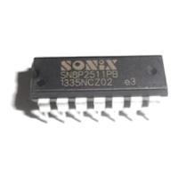
Shows examples of product markings for different package types.
Explains the system used for encoding the date code.
Provides mechanical dimensions for the 14-pin PDIP package.
Provides mechanical dimensions for the 14-pin SOP package.
Provides mechanical dimensions for the 16-pin SSOP package.
| Core Architecture | 8-bit |
|---|---|
| Max Clock Speed | 16 MHz |
| Program Memory Type | Flash |
| Flash Memory | 1 KB |
| RAM | 64 Bytes |
| GPIO Pins | 12 |
| Comparators | 1 |
| Operating Voltage | 2.4V - 5.5V |
| Operating Temperature | -40°C to 85°C |
| Timers | 1 x 8-bit, 1 x 16-bit |