1616
CDX-R3350/R3350C
CDX-R3350/R3350C
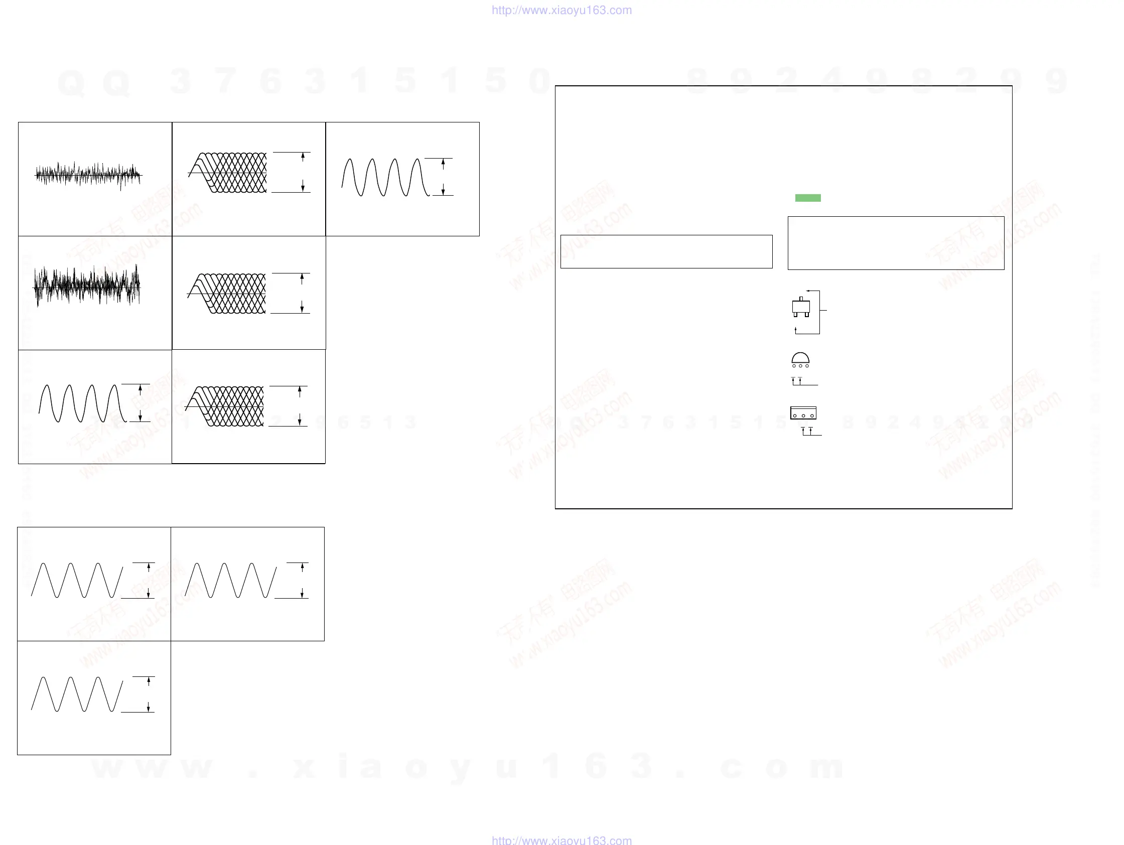
• WAVEFORMS
— MAIN BOARD —
— SERVO BOARD —
(CD PLAY)
1 IC2 4 (FEI)
Approx.
1Vp-p
0 V
0.6 Vp-p
16.9344 MHz
Approx. 100 mVp-p
50 mV/DIV, 5 msec/DIV
0.5 V/DIV, 0.5
µ
sec/DIV
2 IC2 6 (TEI)
200 mV/DIV, 5 msec/DIV
6 IC2 oh (FPI2),
0.5 V/DIV, 0.5
µ
sec/DIV
Approx. 400 mVp-p
3 IC2 wd (XI)
0.2 V/DIV, 0.2
µ
sec/DIV
7 IC3 ia (X1)
0.5 V/DIV, 0.2
µ
sec/DIV
1.1 Vp-p
12 MHz
4 IC2 uj (RFI)
0.5 V/DIV, 0.5
µ
sec/DIV
5 IC2 of (FNI2),
og (FNI1)
1.5 Vp-p
oj (FPI1)
1.5 Vp-p
0 V
1.1 Vp-p
8.664 MHz
1 IC51 9 (XTI)
0.5 V/DIV, 0.2
µ
sec/DIV
0.7 Vp-p
32.768 kHz
2 IC501 ul (X1)
0.2 V/DIV, 20
µ
sec/DIV
2 Vp-p
18.432 MHz
3 IC501 id (OSC IN)
1 V/DIV, 0.1
µ
sec/DIV
• NOTE FOR PRINTED WIRING BOARDS AND SCHEMATIC DIAGRAMS
THIS NOTE IS COMMON FOR PRINTED WIRING
BOARDS AND SCHEMATIC DIAGRAMS.
(In addition to this, the necessary note is printed
in each block.)
For schematic diagrams.
Note:
• All capacitors are in µF unless otherwise noted. (p: pF)
50 WV or less are not indicated except for electrolytics
and tantalums.
• All resistors are in Ω and
1
/
4
W or less unless otherwise
specified.
•
f
: internal component.
• C : panel designation.
For printed wiring boards.
Note:
• X : parts extracted from the component side.
• Y : parts extracted from the conductor side.
•
a
: Through hole.
• : Pattern from the side which enables seeing.
(The other layers' patterns are not indicated.)
• A : B+ Line.
• B : B– Line.
• H : adjustment for repair.
•Voltages and waveforms are dc with respect to ground
under no-signal (detuned) conditions.
• CD mechanism section (1/2), (2/2)
no mark : CD PLAY
• Main (1/3), (2/3), (3/3) and Display sections
no mark : FM
(): MW/LW
<>: CD PLAY
∗ : Impossible to measure
•Voltages are taken with a VOM (Input impedance 10 MΩ).
Voltage variations may be noted due to normal produc-
tion tolerances.
•Waveforms are taken with a oscilloscope.
Voltage variations may be noted due to normal produc-
tion tolerances.
• Circled numbers refer to waveforms.
• Signal path.
J : CD PLAY
F : FM
f : MW/LW
L : BUS AUDIO
Caution:
Pattern face side: Parts on the pattern face side seen from the
(Side B) pattern face are indicated.
Parts face side: Parts on the parts face side seen from the
(Side A) parts face are indicated.
Q
C
These are omitted
EB
E
These are omitted
CB
C
These are omitted
BE
Note: The components identified by mark 0 or dotted line
with mark 0 are critical for safety.
Replace only with part number specified.
w
w
w
.
x
i
a
o
y
u
1
6
3
.
c
o
m
Q
Q
3
7
6
3
1
5
1
5
0
9
9
2
8
9
4
2
9
8
T
E
L
1
3
9
4
2
2
9
6
5
1
3
9
9
2
8
9
4
2
9
8
0
5
1
5
1
3
6
7
3
Q
Q
TEL 13942296513 QQ 376315150 892498299
TEL 13942296513 QQ 376315150 892498299
http://www.xiaoyu163.com
http://www.xiaoyu163.com
 Loading...