3
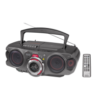
CFD-G550CP
•
UNLEADED SOLDER
Boards requiring use of unleaded solder are printed with the lead-
free mark (LF) indicating the solder contains no lead.
(Caution: Some printed circuit boards may not come printed with
the lead free mark due to their particular size.)
: LEAD FREE MARK
Unleaded solder has the following characteristics.
• Unleaded solder melts at a temperature about 40°C higher than
ordinary solder.
Ordinary soldering irons can be used but the iron tip has to be
applied to the solder joint for a slightly longer time.
Soldering irons using a temperature regulator should be set to
about 350°C.
Caution: The printed pattern (copper foil) may peel away if
the heated tip is applied for too long, so be careful!
• Strong viscosity
Unleaded solder is more viscous (sticky, less prone to flow)
than ordinary solder so use caution not to let solder bridges
occur such as on IC pins, etc.
• Usable with ordinary solder
It is best to use only unleaded solder but unleaded solder may
also be added to ordinary solder.
TABLE OF CONTENTS
1. SERVICING NOTES......................................................... 4
2. GENERAL............................................................................ 5
3. DISASSEMBLY
3-1. Cabinet (Upper) (1) Section ................................................ 9
3-2. Cabinet (Upper) (2) Section ................................................ 9
3-3. Cabinet (Front) Section ..................................................... 10
3-4. Control 2 Board, VOL Board ............................................ 10
3-5. LCD Board ........................................................................ 11
3-6. Power Board, Trans Board ................................................ 11
3-7. Control 1 Board................................................................. 12
3-8. H/P Board, TU Board........................................................ 12
3-9. Main Board ....................................................................... 13
3-10. CD Block Section.............................................................. 13
3-11. Optical Pick-up ................................................................. 14
3-12. Tape Mechanism Deck ...................................................... 14
3-13. TC Board ........................................................................... 15
3-14. Main Belt, Sub Belt ........................................................... 15
4. MECHANICAL ADJUSTMENTS ............................... 16
5. ELECTRICAL ADJUSTMENTS
Tape Section .......................................................................... 16
Tuner Section ......................................................................... 17
CD Section ............................................................................ 18
6. DIAGRAMS
6-1. Block Diagram – CD Section –......................................... 19
6-2. Block Diagram – Main Section – ...................................... 20
6-3. Note for Printed Wiring Boards and
Schematic Diagrams .......................................................... 21
6-4. Waveforms......................................................................... 21
6-5. Circuit Boards Location .................................................... 21
6-6. Printed Wiring Board – CD Section – ............................... 22
6-7. Schematic Diagram – CD Section –.................................. 23
6-8. Printed Wiring Board – Tuner Section – ........................... 24
6-9. Schematic Diagram – Tuner Section – .............................. 25
6-10. Schematic Diagram – Main Section (1/2) – ...................... 26
6-11. Schematic Diagram – Main Section (2/2) – ...................... 27
6-12. Printed Wiring Boards – Main Section – .......................... 28
6-13. Printed Wiring Board – TC Section – ............................... 29
6-14. Schematic Diagram – TC Section – .................................. 30
6-15. Schematic Diagram – Control Section – ........................... 31
6-16. Printed Wiring Boards – Control Section –....................... 32
6-17. Printed Wiring Boards – Power Section –......................... 33
6-18. Schematic Diagram – Power Section – ............................. 34
7. EXPLODED VIEWS
7-1. Overall Section .................................................................. 42
7-2. Cabinet (Front) Section ..................................................... 43
7-3. Cabinet (Rear) Section ...................................................... 44
7-4. Cabinet (Upper) (1) Section .............................................. 45
7-5. Cabinet (Upper) (2) Section .............................................. 46
7-6. Tape Mechanism Section .................................................. 47
7-7. CD Mechanism Section .................................................... 48
8. ELECTRICAL PARTS LIST......................................... 49