40
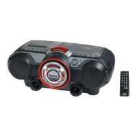
CFD-G550CP
1 TU CE O PLL IC chip enable output
2 TU DATA O PLL IC data output
3 TU CLK O PLL IC clock output
4 TU COUNT I PLL IC IF count data result input
5 TU MUTE O Tuner IF request & mute control output
6 SIMUKE1 I Destination setting pin
7 SIMUKE2 I Destination setting pin
8 TEST B I Audio test mode input
9 VDD — Power supply pin (+3.3V)
10 TEST A I CD/MP3 test mode input
11 EPROM SCL O EEPROM serial clock output
12 EPROM SDA O EEPROM serial data output
13 SIMUKE3 O Destination setting pin
14 to 16 NC O Not used
17 ISS1 O REC bias frequency select output
18 ISS2 O REC bias frequency select output
19 TU ON O RADIO power control signal output
20 TAPE ON O TAPE power control signal output
21 CD ON O CD power control signal output
22 TEST/VPP — Ground
23 to 25 NC O Not used
26 W-LED2 O Woofer LED control signal output
27 W-LED1 O Woofer LED control signal output
28 NC O Not used
29 LCD RST O LCD driver reset output
30 LCD C/D O LCD driver C/D signal output
31 LCD CS O LCD driver chip select output
32 LCD DATA O LCD driver data output
33 LCD CLK O LCD driver clock output
34 NC O Not used
35 FM/AM SHIFT O Oscillator frequency select output
36 NC O Not used
37 VDD — Power supply pin (+3.3V)
38 X2 O Cristal oscillator output (5MHz)
39 X1 I Cristal oscillator input (5MHz)
40 VSS — Ground
41 XT2 O Not used
42 XT1 I Ground
43 RESET I Reset voltage (+2.8V) detect signal input
44 AC CHK I AC/DC check detect signal input
45 RMC IN I Remote control signal input
46 WAKE UP I Wake up signal input
47 NC I Not used
48 CD DOOR I CD door detect signal input
49 INTB (MP3) I Decoder IC interrupt signal input
50 WRQ (CD) I CD interrupt signal input
51 AVDD — Power supply pin (+3.3V)
52 AVREF — Power supply pin (+3.3V)
53 KEY1 I A/D key input 1
54 KEY2 I A/D key input 2
55 KEY3 I A/D key input 3
56 MODEL I Model setting pin
• IC801 µPD784216AGF-546-3BA (SYSTEM CONTROL) (MAIN BOARD (2/2))
Pin No. Pin Name I/O Pin Description