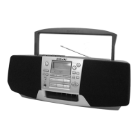
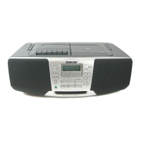
CFD-S45L/S47L
– 27 – – 28 –
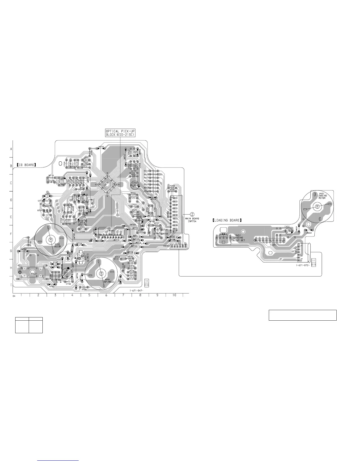
5-7. PRINTED WIRING BOARDS — CD SECTION — • Refer to page 18 for Circuit Boards Location.
IC701 F-6
IC702 H-2
Q701 E-2
• Semiconductor
Location
Ref. No. Location
Note on Printed Wiring Boards:
• X : parts extracted from the component side.
• b : Pattern from the side which enables seeing.
Note on Schematic Diagram:
• All capacitors are in µF unless otherwise noted. pF: µµF
50 WV or less are not indicated except for electrolytics
and tantalums.
• All resistors are in Ω and
1
/
4
W or less unless otherwise
specified.
Note: The components identified by mark ! or dotted line
with mark ! are critical for safety.
Replace only with part number specified.
• U : B+ Line.
• Voltage and waveforms are dc with respect to ground
under no-signal (detuned) conditions.
no mark : CD STOP
• Voltages are taken with a VOM (Input impedance 10 MΩ).
Voltage variations may be noted due to normal produc-
tion tolerances.
• Circled numbers refer to waveforms.
• Signal path.
J : CD
(Page 34)