– 35 – – 36 – – 37 –
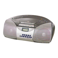
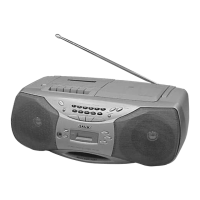
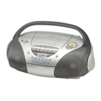
CFD-S45L/S47L
5-10. SCHEMATIC DIAGRAM — MAIN SECTION (1/2) — • Refer to page 41 for IC Block Diagrams.
• Semiconductor
Location
(MAIN Board)
Ref. No. Location
D302 G-13
D350 F-3
D351 B-4
D352 C-2
D353 C-8
D354 B-3
D355 A-7
D356 A-8
D357 C-6
D358 B-11
D501 P-2
D502 P-2
D503 Q-2
D504 Q-2
D505 Q-14
D506 Q-14
D507 M-12
D508 M-12
IC301 G-11
IC302 F-8
IC305 C-12
IC306 C-9
IC501 O-6
IC502 N-3
IC503 P-10
IC703 L-10
Q301 H-14
Q302 F-14
Q303 F-14
Q304 H-14
Q341 D-7
Q342 B-11
Q351 C-2
Q352 D-1
Q353 D-6
Q354 B-8
Q355 D-5
Q356 D-1
Q357 D-1
Q358 C-1
Q359 B-7
Q360 J-5
Q368 I-13
Q369 I-14
Q501 R-3
Q502 R-4
Q503 R-4
Q504 R-5
Q505 Q-13
Q506 Q-13
Q507 Q-4
Q508 Q-4
Q509 Q-13
Note:
• All capacitors are in µF unless otherwise noted. pF: µµF
50 WV or less are not indicated except for electrolytics
and tantalums.
• All resistors are in Ω and
1
/
4
W or less unless otherwise
specified.
• C : panel designation.
• U : B+ Line.
• Voltage is dc with respect to ground under no-signal
(detuned) condition.
no mark : COMMON
( ) : TAPE (PB)
< > : TAPE (REC)
[ ] : CD STOP
• Signal path.
F : FM
d : PB
G : REC
J : CD
Note: The components identified by mark ! or dotted line
with mark ! are critical for safety.
Replace only with part number specified.
(Page 31)
(Page 38)
(Page 26)
(Page 39)
(Page 30, 39)