– 23 – – 24 – – 26 –– 25 –
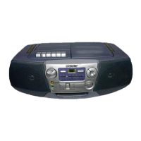
CFD-V5
6-4. SCHEMATIC DIAGRAM – MAIN SECTION (1/2) –
Note:
• All capacitors are in µF unless otherwise noted. pF: µµF
50 WV or less are not indicated except for electrolytics
and tantalums.
• All resistors are in Ω and
1
/
4
W or less unless otherwise
specified.
•
f
: internal component.
Note: The components identified by mark 0 or dotted
line with mark 0 are critical for safety.
Replace only with part number specified.
• U : B+ Line.
• H : adjustment for repair.
• Power voltage is dc 9V and fed with regulated dc power
supply from battery terminal.
• Voltages and waveforms are dc with respect to ground
under no-signal (detuned) conditions.
no mark :FM (RADIO SECTION),
PLAY (TAPE SECTION)
( ) :AM (RADIO SECTION),
REC (TAPE SECTION)
• Voltages are taken with a VOM (Input impedance 10 MΩ).
Voltage variations may be noted due to normal produc-
tion tolerances.
• Waveforms are taken with a oscilloscope.
Voltage variations may be noted due to normal produc-
tion tolerances.
• Signal path.
F : FM
f : AM
E : PB
a : REC
J : CD
z
Refer to page 30 - 31 for IC Block Diagrams.
1
2
Q301 C
T301
VOLT/DIV : 1 V AC
TIME/DIV : 5 µsec
VOLT/DIV : 1 V AC
(ATT : 1/10)
TIME/DIV : 5 µsec
r
Waveforms
3.7Vp-