DCR-TRV255E/TRV260/TRV265/TRV265E
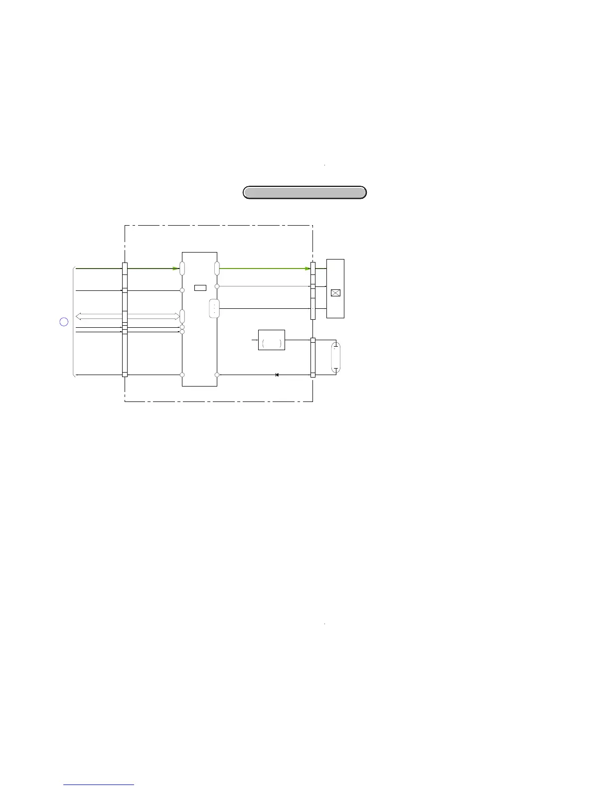
3. BLOCK DIAGRAMS
3. BLOCK DIAGRAMS
VD SO, VD SI, VD SCK VD SO, VD SI, VD SCK
PD-204 BOARD (2/2)
05
IC6001
LCD
DRIVER
VCOM
N.C./SPC, GRES/EX1, GPCK/MO1, GSRT/MO2,
STBYB/PSG,RESET/EX2, VBC/CLS, STBYB/RES,
SRT/PSS1, OE/PSS2, CLR/CTR, MCLK/CLD, HCNT/SPD
VR, VG, VB
2.5 INCH
COLOR
LCD UNIT
LCD901
CN6004
CN6003
40
ı
38
19
ı
21
23
30
INVERTER
TRANSFORMER
BACKLIGHT
DRIBE
T6001, Q6002
ND901
BACKLIGHT
BL HIGH
BL LOW
BL DET
45
42
43
46
ı
48
28
11
19
ı
21
5
ı
10
12
ı
18
BL REG
10
3
CN6001
(2/2)
XCS LCD DA
PANEL R, PANEL G, PANEL BPANEL R, PANEL G, PANEL B
XCS LCD DA
PANEL XVD
BL CONT BL CONT
OVERALL (2/5)
(PAGE 3-4)
C-SYNC/XHD
D6004
12
10
7
ı
5
8
4
11
ı
13
PANEL XVD
C-SYNC/XHD
9
A : VIDEO SIGNAL
2–6
14–16
29
32–35
TYPE C/S: Please refer to page 1-3
to discriminate the type of LCD.
NOTE: CN6004 Pin Name A/B
A: TYPE C MODEL
B: TYPE S MODEL
3-9 3-10
3-5. OVERALL BLOCK DIAGRAM (5/5)
( ) : Number in parenthesis ( ) indicates the division number of schematic diagram where the component is located.
 Loading...